|
|
|
PDF NB3N106K Data sheet ( Hoja de datos )
| Número de pieza | NB3N106K | |
| Descripción | 3.3V Differential 1:6 Fanout Clock Driver | |
| Fabricantes | ON Semiconductor | |
| Logotipo | ||
Hay una vista previa y un enlace de descarga de NB3N106K (archivo pdf) en la parte inferior de esta página. Total 10 Páginas | ||
|
No Preview Available !
NB3N106K
3.3V Differential 1:6 Fanout
Clock Driver with HCSL
Outputs
Description
The NB3N106K is a differential 1:6 Clock fanout buffer with
High−speed Current Steering Logic (HCSL) outputs optimized for
ultra low propagation delay variation. The NB3N106K is designed
with HCSL PCI Express clock distribution and FBDIMM
applications in mind.
Inputs can directly accept differential LVPECL, LVDS, and HCSL
signals per Figures 7, 8, and 9. Single−ended LVPECL, HCSL,
LVCMOS, or LVTTL levels are accepted with a proper external Vth
reference supply per Figures 4 and 10. Input pins incorporate separate
internal 50 W termination resistors allowing additional single ended
system interconnect flexibility.
Output drive current is set by connecting a 475 W resistor from
IREF (Pin 1) to GND per Figure 6. Outputs can also interface to
LVDS receivers when terminated per Figure 11.
The NB3N106K specifically guarantees low output–to–output
skew. Optimal design, layout, and processing minimize skew within a
device and from device to device. System designers can take
advantage of the NB3N106K’s performance to distribute low skew
clocks across the backplane or the motherboard.
Features
• Typical Input Clock Frequency 100, 133, 166, 200, 266, 333, and
400 MHz
• 220 ps Typical Rise and Fall Times
• 800 ps Typical Propagation Delay
• Dtpd 100 ps Maximum Propagation Delay Variation per Diff Pair
• 0.1 ps Typical Integrated Phase Jitter RMS
• Operating Range: VCC = 3.0 V to 3.6 V with VEE = 0 V
• Typical HCSL Output Levels (700 mV Peak−to−Peak)
• LVDS Output Levels with Interface Termination
• These are Pb−Free Devices*
Applications
• Clock Distribution
• PCIe, II, III
• Networking and Communications
• High End Computing
End Products
• Servers
• FBDIMM Memory Cards
• Ethernet Switch/Routers
*For additional information on our Pb−Free strategy and soldering details, please
download the ON Semiconductor Soldering and Mounting Techniques
Reference Manual, SOLDERRM/D.
http://onsemi.com
QFN−24
MN SUFFIX
CASE 485L
MARKING DIAGRAM*
NB3N
106K
ALYWG
G
A = Assembly Location
L = Wafer Lot
Y = Year
W = Work Week
G = Pb−Free Package
*For additional marking information, refer to
Application Note AND8002/D.
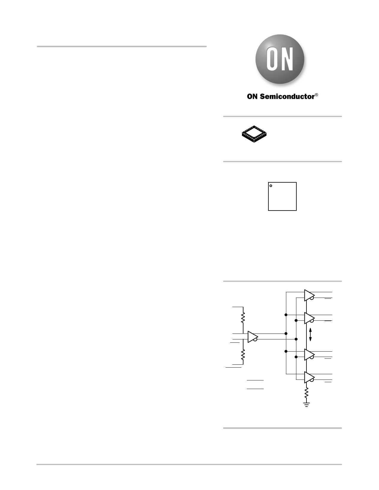
VTCLK
Q0
Q0
Q1
CLK Q1
CLK
VTCLK
VCC
GND
IREF
RREF
Q4
Q4
Q5
Q5
Figure 1. Simplified Logic Diagram
ORDERING INFORMATION
See detailed ordering and shipping information in the
package dimensions section on page 9 of this data sheet.
© Semiconductor Components Industries, LLC, 2012
April, 2012 − Rev. 5
1
Publication Order Number:
NB3N106K/D
1 page 
NB3N106K
Table 5. AC CHARACTERISTICS VCC = 3.0 V to 3.6 V, GND = 0 V; −40°C to +85°C (Note 6)
Symbol
Characteristic
Min Typ Max Unit
VOUTPP
tPLH,
tPHL
DtPLH,
DtPHL
tSKEW
Output Voltage Amplitude (@ VINPPmin) fin ≤ 400 MHz
Propagation Delay (See Figure 3a)
CLK/CLK to Qx/Qx
Propagation Delay Variation Per Each Diff Pair (Note 7) (See Figure 3a)
CLK/CLK to Qx/Qx
Duty Cycle Skew (Note 8)
Within -Device Skew
Device to Device Skew (Note 9)
550
725 1000 mV
800 1100 ps
ps
100
20 ps
100
150
tJITq
VINPP
Integrated Phase Jitter RMS (Note 10)
Input Voltage Swing/Sensitivity
(Differential Configuration)
0.1 ps
0.150
VCC −
0.85
V
VCROSS
DVCROSS
tr , tf
Absolute Crossing Magnitude Voltage (See Figure 3b)
Variation in Magnitude of VCROSS (See Figure 3b)
Absolute Magnitude in Output Risetime and Falltime (from 175 mV to 525 mV)
(See Figure 3b)
250
Qx, Qx 150
550
150
220 400
mV
mV
ps
Dtr, Dtf Variation in Magnitude of Risetime and Falltime (Single−Ended) at VCC = 3.0 V, 3.3 V,
3.6 V (See Figure 3b)
Qx, Qx
ps
125
NOTE: Device will meet the specifications after thermal equilibrium has been established when mounted in a test socket or printed circuit
board with maintained transverse airflow greater than 500 lfpm. Electrical parameters are guaranteed only over the declared
operating temperature range. Functional operation of the device exceeding these conditions is not implied. Device specification limit
values are applied individually under normal operating conditions and not valid simultaneously.
6. Measured by forcing VINPP (MIN) from a 50% duty cycle clock source. Measurements taken all outputs loaded 50 W to GND per Figure 6.
Connect a 475 W resistor from IREF (Pin 1) to GND. See Figure 6.
7. Measured from the input pair crosspoint to each single output pair crosspoint across temp and voltage ranges per Figure 3.
8. Duty cycle skew is measured between differential outputs using the deviations of the sum of Tpw- and Tpw+.
9. Skew is measured between outputs under identical transition conditions @ 50 MHz.
10. Phase noise integrated from 12 kHz to 20 MHz.
http://onsemi.com
5
5 Page | ||
| Páginas | Total 10 Páginas | |
| PDF Descargar | [ Datasheet NB3N106K.PDF ] | |
Hoja de datos destacado
| Número de pieza | Descripción | Fabricantes |
| NB3N106K | 3.3V Differential 1:6 Fanout Clock Driver | ON Semiconductor |
| Número de pieza | Descripción | Fabricantes |
| SLA6805M | High Voltage 3 phase Motor Driver IC. |
Sanken |
| SDC1742 | 12- and 14-Bit Hybrid Synchro / Resolver-to-Digital Converters. |
Analog Devices |
|
DataSheet.es es una pagina web que funciona como un repositorio de manuales o hoja de datos de muchos de los productos más populares, |
| DataSheet.es | 2020 | Privacy Policy | Contacto | Buscar |