|
|
|
PDF 96S02 Data sheet ( Hoja de datos )
| Número de pieza | 96S02 | |
| Descripción | DM96S02 | |
| Fabricantes | Fairchild Semiconductor | |
| Logotipo | ||
Hay una vista previa y un enlace de descarga de 96S02 (archivo pdf) en la parte inferior de esta página. Total 7 Páginas | ||
|
No Preview Available !
January 1992
Revised June 1999
DM96S02
Dual Retriggerable Resettable Monostable Multivibrator
General Description
The DM96S02 is a dual retriggerable and resettable
w
w
w
.
D
a
t
a
S
h
e
mteioonntaolls4ytawbUildee.mdeucllatiyvoibrarmantgoer.,
This one-shot provides excep-
pulse width stability, predictable
accuracy and immunity to noise. The pulse width is set by
an external resistor and capacitor. Resistor values up to 2.0
MΩ for the DM96S02 reduce required capacitor values.
Hysteresis is provided on the positive trigger input of the
DM96S02 for increased noise immunity.
Order Code:
Order Number Package Number
Package Description
DM96S02M
M16A
16-Lead Small Outline Integrated Circuit (SOIC), JEDEC MS-012, 0.150 Narrow
DM96S02N
N16E
16-Lead Plastic Dual-In-Line Package (PDIP), JEDEC MS-001, 0.300 Wide
Devices also available in Tape and Reel. Specify by appending the suffix letter “X” to the ordering code.
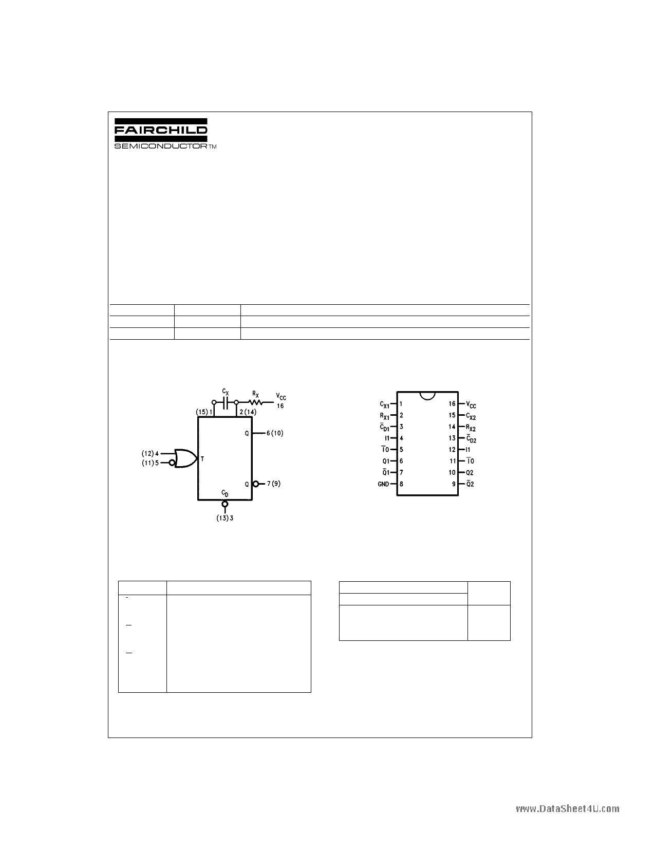
Logic Diagram
Connection Diagram
VCC = Pin 16
GND = Pin 8
Pin Descriptions
Pin Names
Description
I0 Trigger Input (Active Falling Edge)
I1 Schmitt Trigger Input (Active Rising-Edge)
CD
Q1 - 2
Direct Clear Input (Active-LOW)
True Pulse Output
Q1 - 2
Complementary Pulse Output
CX1, 2
RX1,2
External Capacitor Connection
External Resistor Connection
Triggering Truth Table
Pin Number
5(11)
4(12)
3(13)
H→L
L
H
H L→H H
XXL
H = HIGH Voltage Level ≥ VIH
L = LOW Voltage Level ≤ VIL
X = Immaterial (either H or L)
H → L = HIGH-to-LOW Voltage Level transition
L → H = LOW-to-HIGH Voltage Level transition
Operation
Trigger
Trigger
Reset
© 1999 Fairchild Semiconductor Corporation DS009810.prf
www.fairchildsemi.com
1 page 
www.DataSheet4U.com
AC Electrical Characteristics
VCC = +5.0, TA = +25°C (See Section for Waveforms and Load Configurations)
Symbol
Parameter
Conditions
tPLH
tPHL
tPLH
tPHL
tPHL
tPLH
tW(L)
tW(H)
tW(L)
tW(H)
tW
RX
t∆t
t∆t
Propagation Delay
I0 to Q
Propagation Delay
I0 to Q
Propagation Delay
I1 to Q
Propagation Delay
I1 to Q
Propagation Delay
CD to Q
Propagation Delay
CD to Q
I0 Pulse Width LOW
I1 Pulse Width HIGH
CD Pulse Width LOW
Minimum Q Pulse Width HIGH
Q Pulse Width
Timing Resistor Range (Note 3)
Change in Q Pulse Width
over Temperature
Change in Q Pulse Width
over VCC Range
Note 3: Applies only over VCC and TX range for DM96S02.
Note 4: All Typicals are at VCC = 5V, TA = 25°C
Figure 1
RX = 1.0 kΩ, CX = 10 pF
Including Jig and Stray
RX = 10 kΩ, CX = 1000 pF
TA = −55°C to + 125°C
VCC = 4.5V to 5.5V
RX = 10 kΩ, CX = 1000 pF
TA = 25°C, VCC = 4.75V to
5.25V, RX = 10 kΩ,
CX = 1000 pF
TA = 25°C, VCC = 4.5 to
5.5V, RX = 10 kΩ,
CX = 1000 pF
Switching Waveforms
CL = 16 pF
Min Max
15
19
19
20
20
14
8.0
12
7.0
30 45
5.2 5.8
1.0 2000
1.0
Units
ns
ns
ns
ns
ns
ns
ns
ns
ns
ns
µs
kΩ
%
1.0 %
FIGURE 1.
5
www.fairchildsemi.com
5 Page | ||
| Páginas | Total 7 Páginas | |
| PDF Descargar | [ Datasheet 96S02.PDF ] | |
Hoja de datos destacado
| Número de pieza | Descripción | Fabricantes |
| 96S02 | DM96S02 | Fairchild Semiconductor |
| Número de pieza | Descripción | Fabricantes |
| SLA6805M | High Voltage 3 phase Motor Driver IC. |
Sanken |
| SDC1742 | 12- and 14-Bit Hybrid Synchro / Resolver-to-Digital Converters. |
Analog Devices |
|
DataSheet.es es una pagina web que funciona como un repositorio de manuales o hoja de datos de muchos de los productos más populares, |
| DataSheet.es | 2020 | Privacy Policy | Contacto | Buscar |