|
|
|
PDF LTC3534 Data sheet ( Hoja de datos )
| Número de pieza | LTC3534 | |
| Descripción | 500mA Synchronous Buck-Boost DC/DC Converter | |
| Fabricantes | Linear | |
| Logotipo | ||
Hay una vista previa y un enlace de descarga de LTC3534 (archivo pdf) en la parte inferior de esta página. Total 20 Páginas | ||
|
No Preview Available !
Features
n Regulated Output with Input Voltages Above,
Below or Equal to the Output
n 2.4V to 7V VIN and 1.8V to 7V VOUT Ranges
n 5V VOUT at 500mA from 4 AA Cells
n Single Inductor
n Synchronous Rectification: Up to 94% Efficiency
n Burst Mode® Operation with 25µA IQ
n Output Disconnect in Shutdown
n 1MHz Switching Frequency
n <1µA Shutdown Current
n Small Thermally Enhanced 16-Lead (5mm × 3mm ×
0.75mm) DFN and 16-Lead GN Packages
Applications
n Medical Instruments
n Portable Barcode Readers
n Portable Inventory Terminals
n USB to 5V Supply
n Handheld GPS
LTC3534
7V, 500mA Synchronous
Buck-Boost DC/DC
Converter
Description
The LTC®3534 is a wide VIN range, highly efficient, fixed
frequency, buck-boost DC/DC converter that operates
from input voltages above, below or equal to the output
voltage. The topology incorporated in the IC provides a
continuous transfer function through all operating modes,
making the product ideal for multi-cell Alkaline/NiMH or
single Lithium-Ion/Polymer applications where the output
voltage is within the battery voltage range.
The LTC3534 offers extended VIN and VOUT ranges of 2.4V
to 7V and 1.8V to 7V, respectively. Quiescent current is
only 25µA in Burst Mode operation, maximizing battery
life in portable applications. Burst Mode operation is user
controlled and can be enabled by driving the PWM pin
low. If the PWM pin is driven high then fixed frequency
switching is enabled.
Other features include fixed 1MHz operating frequency, a
<1µA shutdown, short-circuit protection, programmable
soft-start, current limit and thermal overload protection.
The LTC3534 is available in the thermally enhanced 16-lead
(3mm × 5mm) DFN and 16-lead GN packages.
L, LT, LTC and LTM are registered trademarks of Linear Technology Corporation.
Burst Mode is a registered trademark of Linear Technology Corporation.
All other trademarks are the property of their respective owners.
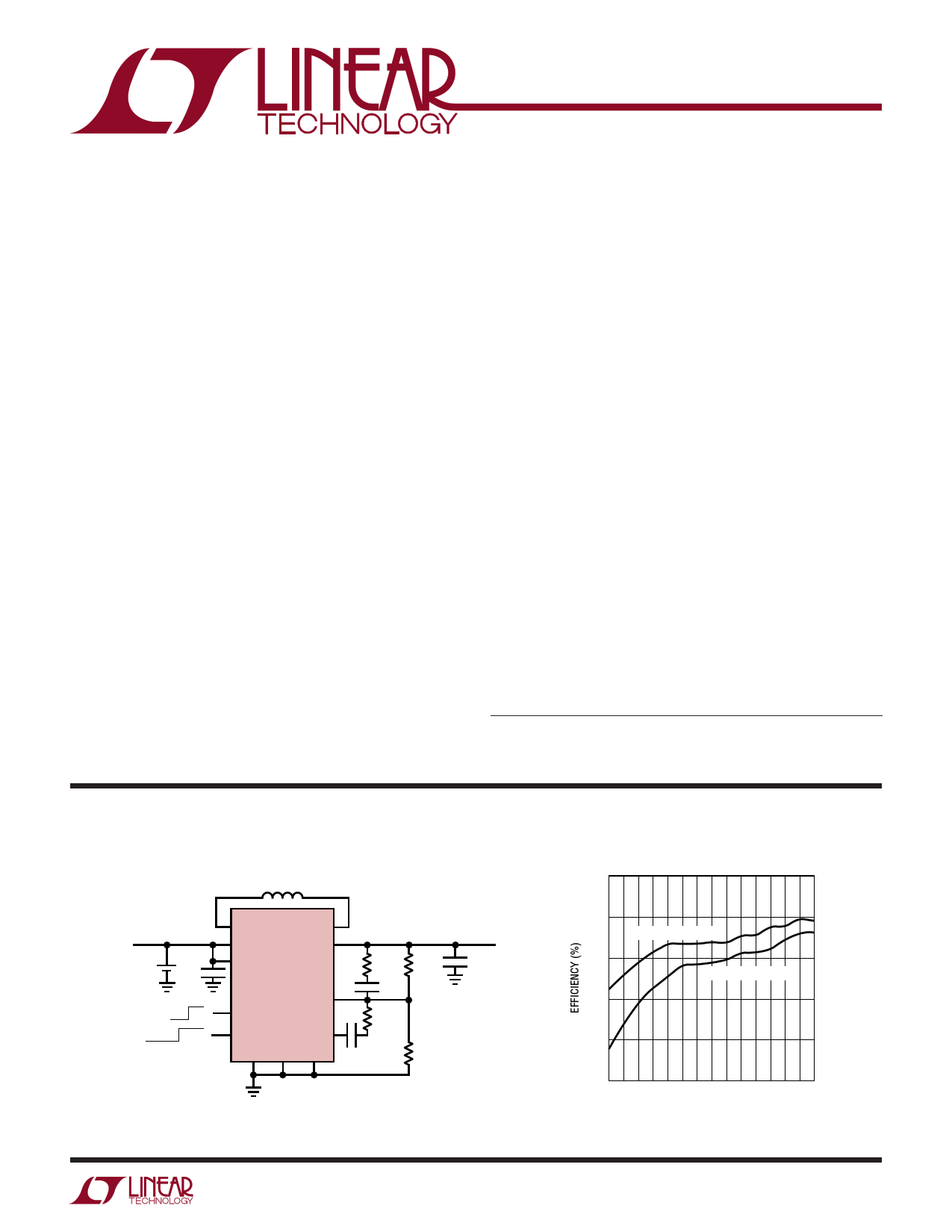
Typical Application
4 AA Cells to 5V at 500mA Buck-Boost Converter
5µH
VIN
3.6V TO 6.4V 4 AA +
CELLS
10µF
OFF ON
BURST PWM
SW1 SW2
PVIN
VOUT
VIN
LTC3534
RUN/SS
FB
10k
33pF
15k
PWM
VC
PGND1 GND PGND2 330pF
649k
162k
3534 TA01a
VOUT
5V
22µF 500mA
4 AA Cells to 5V Efficiency vs VIN
100
95
PWM IOUT = 300mA
90
PWM IOUT = 500mA
85
80
75
3.6 4.0 4.4 4.8 5.2 5.6 6.0 6.4
VIN (V)
3534 TA01b
For more information www.linear.com/LTC3534
3534fb
1
1 page 
LTC3534
Typical Performance Characteristics TA = 25°C, unless otherwise noted.
Converter Line Regulation
vs Temperature
5.005 ILOAD = 100mA
5.000
4.995
4.990
4.985
4.980
4.975
–50
–25 0 25 50
TEMPERATURE (°C)
3.6V
5.0V
6.4V
75 100
3534 G08
Switching Frequency
vs Temperature
1050
1025
1000
975
950
–50
–25 0 25 50
TEMPERATURE (°C)
75 100
3534 G11
PWM No-Load Input Current
vs VIN (Switching)
18 VOUT = 5V
14
10
6
2
2.4 3.2
4 4.8 5.6 6.4
INPUT VOLTAGE (V)
7.2 8
3534 G14
Converter Load Regulation
vs Temperature
5.01 VIN = 5V
5.00
25mA
4.99 300mA
4.98
500mA
4.97
4.96
4.95
–50
–25 0 25 50
TEMPERATURE (°C)
75 100
3534 G09
Current Limits vs Temperature
3.0 VIN = VOUT = 5V
2.8
PEAK CURRENT LIMIT
2.5
2.3
2.0
LINEAR CURRENT LIMIT
1.8
1.5
–50
–25 0 25 50
TEMPERATURE (°C)
75 100
3534 G12
BURST Maximum Output Current
Capability vs VIN
200
175
150
125
100
75
VOUT = 5V
50 Burst Mode OPERATION
2.4 3.2 4 4.8 5.6
6.4
INPUT VOLTAGE (V)
7.2 8
3534 G15
For more information www.linear.com/LTC3534
Feedback Voltage vs Temperature
1.001
1.000
0.999
0.998
0.997
–50
–25 0 25 50
TEMPERATURE (°C)
75 100
3534 G10
BURST No-Load Input Current
vs VIN (Switching)
50 VOUT = 5V
45
40
35
30
2.4 3.2
4 4.8 5.6 6.4
INPUT VOLTAGE (V)
7.2 8
3534 G13
PWM Maximum Output Current
Capability vs VIN
1800
VOUT = 5V
1600 L = 4.7µH
1400
1200
1000
800
600
400
200
2.4 3.2
4 4.8 5.6 6.4
INPUT VOLTAGE (V)
7.2 8
3534 G16
3534fb
5
5 Page 
LTC3534
Operation
In Burst Mode operation the typical maximum average
output currents in the three operating regions, buck, four
switch, and boost are given by:
IOUT(MAX)BURST–BUCK ≈ 100mA;
Burst Mode operation – buck region: VIN > VOUT
IOUT(MAX)BURST–FOUR_SWITCH ≈ 125mA;
Burst Mode operation – four switch region: VIN ≈ VOUT
IOUT(MAX )BURST −BOOST
≈
125 • VIN
VOUT
mA;
Burst Mode operation – boost region: VIN < VOUT
The efficiency below 1mA becomes dominated primarily
by the quiescent current. The Burst Mode operation ef-
ficiency is given by:
Efficiency
≅
η •ILOAD
25µA +ILOAD
where h is typically 90% during Burst Mode operation.
A graph of Burst Mode operation maximum output current
vs VIN (for VOUT = 5V) is provided in the Typical Perfor-
mance Characteristics section.
Burst Mode Operation to Fixed Frequency Transient
Response
In Burst Mode operation, the compensation network is
not used and VC is disconnected from the error amplifier.
During long periods of Burst Mode operation, leakage
currents in the external components or on the PC board
could cause the compensation capacitor to charge (or
discharge), which could result in a large output transient
when returning to fixed frequency mode operation, even
at the same load current. To prevent this, the LTC3534
incorporates an active clamp circuit that holds the voltage
on VC at an optimal voltage during Burst Mode operation.
This minimizes any output transient when returning to
fixed frequency mode operation. For optimum transient
response, Type III compensation is also recommended
to broad band the control loop and roll off past the two
pole response of the output LC filter. (See Closing the
Feedback Loop).
Soft-Start
The soft-start function is combined with shutdown. When
the RUN/SS pin is brought above 1V typical, the LTC3534
is enabled but the error amplifier duty cycle is clamped
from VC. A detailed diagram of this function is shown in
Figure 3. The components RSS and CSS provide a slow
ramping voltage on RUN/SS to provide a soft-start func-
tion. To ensure that VC is not being clamped, RUN/SS
must be raised to 2.4V or above. The IC must be enabled
(even with a soft-start) commanding PWM mode. Once
the LTC3534 is in regulation, then Burst Mode operation
can be commanded.
ENABLE
SIGNAL
RSS
RUN/SS
2
CSS
VIN
13
CHIP
ENABLE
+
– 1V
+
ERROR
AMP
–
1V
FB
15
VCI TO PWM
COMPARATORS
VC CP1
14
VOUT
11
R1
R2
3534 F03
Figure 3. Soft-Start Circuitry
For more information www.linear.com/LTC3534
3534fb
11
11 Page | ||
| Páginas | Total 20 Páginas | |
| PDF Descargar | [ Datasheet LTC3534.PDF ] | |
Hoja de datos destacado
| Número de pieza | Descripción | Fabricantes |
| LTC3530 | Wide Input Voltage Synchronous Buck-Boost DC/DC Converter | Linear Technology |
| LTC3531 | Buck-Boost Synchronous DC/DC Converters | Linear Technology |
| LTC3531-3 | Buck-Boost Synchronous DC/DC Converters | Linear Technology |
| LTC3531-3.3 | Buck-Boost Synchronous DC/DC Converters | Linear Technology |
| Número de pieza | Descripción | Fabricantes |
| SLA6805M | High Voltage 3 phase Motor Driver IC. |
Sanken |
| SDC1742 | 12- and 14-Bit Hybrid Synchro / Resolver-to-Digital Converters. |
Analog Devices |
|
DataSheet.es es una pagina web que funciona como un repositorio de manuales o hoja de datos de muchos de los productos más populares, |
| DataSheet.es | 2020 | Privacy Policy | Contacto | Buscar |