|
|
|
PDF LT8570-1 Data sheet ( Hoja de datos )
| Número de pieza | LT8570-1 | |
| Descripción | Boost/SEPIC/Inverting DC/DC Converter | |
| Fabricantes | Linear | |
| Logotipo | ||
Hay una vista previa y un enlace de descarga de LT8570-1 (archivo pdf) en la parte inferior de esta página. Total 30 Páginas | ||
|
No Preview Available !
LT8570/LT8570-1
Boost/SEPIC/Inverting
DC/DC Converter with 65V
Switch, Soft-Start and Synchronization
Features
n 65V Power Switch
n Current Limit Options of 0.5A (LT8570) or 0.25A
(LT8570-1)
n Adjustable Switching Frequency
n Single Feedback Resistor Sets VOUT
n Synchronizable to External Clock
n High Gain SHDN Pin Accepts Slowly Varying
Input Signals
n Wide Input Voltage Range: 2.55V to 40V
n Low VCESAT Switch
n Integrated Soft-Start Function
n Easily Configurable as a Boost, SEPIC, or Inverting
Converter
n User Configurable Undervoltage Lockout (UVLO)
n Pin Compatible with LT3580 and LT8580
n Tiny Thermally Enhanced 8-Lead 3mm × 3mm DFN
and 8-Lead MSOP Packages
Applications
n VFD Bias Supplies
n TFT-LCD Bias Supplies
n GPS Receivers
n DSL Modems
n Local Power Supply
Description
The LT®8570 and LT8570-1 are PWM DC/DC converters.
The LT8570 contains a 0.5A, 65V power switch, while
the LT8570-1 contains a 0.25A, 65V power switch. The
LT8570 and LT8570-1 can be configured as either a boost,
SEPIC or inverting converter.
The LT8570/LT8570-1 have an adjustable oscillator, set
by a resistor from the RT pin to ground. Additionally, the
LT8570/LT8570-1 can be synchronized to an external
clock. The switching frequency of the part may be free
running or synchronized, and can be set between 200kHz
and 1.5MHz.
The LT8570/LT8570-1 also feature innovative SHDN pin
circuitry that allows for slowly varying input signals and
an adjustable undervoltage lockout function.
Additional features such as frequency foldback and soft-
start are integrated. The LT8570/LT8570-1 are available
in tiny thermally enhanced 3mm × 3mm 8-lead DFN and
8-lead MSOP packages.
L, LT, LTC, LTM, Linear Technology and the Linear logo are registered trademarks and
ThinSOT is a trademark of Linear Technology Corporation. All other trademarks are the
property of their respective owners. Protected by U.S. Patents, including 7579816.
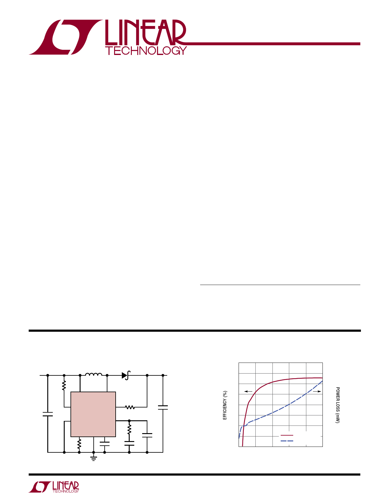
Typical Application
1.5MHz, 5V to 12V Boost Converter
VIN 22µH
5V
10k
VOUT
12V
125mA
VIN
SHDN
SW
FBX
130k
1µF LT8570
SYNC
VC
2.2µF
RT GND SS
6.19k
47pF
56.2k
0.1µF
2.2nF
8570 TA01a
100
90
80
70
60
50
40
30
20
0
Efficiency and Power Loss
320
280
240
200
160
120
80
EFFICIENCY 40
POWER LOSS
0
25 50 75 100 125
LOAD CURRENT (mA)
8570 TA01b
For more information www.linear.com/LT8570
85701f
1
1 page 
LT8570/LT8570-1
Typical Performance Characteristics TA = 25°C, unless otherwise specified
Oscillator Frequency During
Soft-Start
1
1/2
1/3
1/4
1/5
1/6 INVERTING
NONINVERTING
CONFIGURATIONS CONFIGURATIONS
0
0 0.2 0.4 0.6 0.8 1
FBX VOLTAGE (V)
1.2
8570 G08
Internal UVLO
2.7
2.6
2.5
2.4
2.3
2.2
2.1
–50 –25
0 25 50 75 100 125 150
TEMPERATURE (°C)
8570 G09
SHDN Pin Current
30
125°C
25°C
25 –40°C
20
15
10
5
0
0 0.25 0.5 0.75 1 1.25 1.5 1.75 2
SHDN VOLTAGE (V)
8570 G10
SHDN Pin Current
400
125°C
350 25°C
–40°C
300
250
200
150
100
50
0
0 5 10 15 20 25 30 35 40
SHDN VOLTAGE (V)
8570 G11
Active/Lockout Threshold
1.40
1.38
1.36
1.34
1.32 SHDN RISING
1.30
1.28
1.26 SHDN FALLING
1.24
1.22
1.20
–50 –25
0 25 50 75 100 125 150
TEMPERATURE (°C)
8570 G12
Minimum On-Time vs Temperature
280
240
RECOMMENDED MINIMUM ON-TIME
200
160
120
80 MEASURED MINIMUM ON-TIME
40
0
–50 –25
0 25 50 75 100 125 150
TEMPERATURE (°C)
8570 G13
For more information www.linear.com/LT8570
85701f
5
5 Page 
LT8570/LT8570-1
Applications Information
and (2) avoiding subharmonic oscillation. Choose an
inductance that is high enough to meet both of these
requirements.
Adequate Load Current : Small value inductors result in
increased ripple currents and thus, due to the limited peak
switch current, decrease the average current that can be
provided to a load (IOUT). In order to provide adequate
load current, L should be at least:
LBOOST
>
2
•
f
•
DC • VIN
⎛
⎝⎜
ILIM
−
|VOUT|
VIN
• IOUT
•η
⎞
⎠⎟
for boost, topologies, or:
LDUAL
>
DC • VIN
2
•
f
•
⎛
⎝⎜
ILIM−
VOUT
VIN
• IOUT
•η
−
IOUT
⎞
⎠⎟
for the SEPIC and inverting topologies.
where:
LBOOST = L1 for boost topologies (see Figure 15)
LDUAL = L1 = L2 for coupled dual inductor topologies
(see Figure 16 and Figure 17)
LDUAL = L1||L2 for uncoupled dual inductor topologies
(see Figure 16 and Figure 17)
DC = switch duty cycle (see previous section)
ILIM = switch current limit, typically about 0.6A for
LT8570 and 0.3A for LT8570-1 at 50% duty cycle (see
the Typical Performance Characteristics section).
h = power conversion efficiency (typically 85% for boost
and 83% for dual inductor topologies at high currents).
f = switching frequency
IOUT = maximum load current
Negative values of L indicate that the output load current
IOUT exceeds the switch current limit capability of the
LT8570/LT8570-1.
Avoiding Subharmonic Oscillations: The LT8570/
LT8570-1’s internalslopecompensation circuitcanprevent
subharmonic oscillations that can occur when the duty cycle
is greater than 50%, provided that the inductance exceeds
a minimum value. In applications that operate with duty
cycles greater than 50%, the inductance must be at least:
LMIN
>
kSC
VIN
• (DC − 300ns • f) •
f
i
2 i DC − 1
1− DC
LMIN = L1 for boost topologies (see Figure 15)
LMIN = L1 = L2 for coupled dual inductor topologies
(see Figure 16 and Figure 17)
LMIN = L1||L2 for uncoupled dual inductor topologies
(see Figure 16 and Figure 17)
kSC = 0.6 for LT8570 and 0.3 for LT8570-1
Maximum Inductance: Excessive inductance can reduce
current ripple to levels that are difficult for the current com-
parator (A3 in the Block Diagram) to cleanly discriminate,
thus causing duty cycle jitter and/or poor regulation. The
maximum inductance can be calculated by:
LMAX
=
VIN − VCESAT
IMIN-RIPPLE
•
DC
f
where
LMIN = L1 for boost topologies (see Figure 15)
LMIN = L1 = L2 for coupled dual inductor topologies
(see Figure 16 and Figure 17)
LMIN = L1||L2 for uncoupled dual inductor topologies
(see Figure 16 and Figure 17)
IMIN-RIPPLE = typically 40mA for LT8570 and 20mA for
LT8570-1
Current Rating: Finally, the inductor(s) must have a rating
greater than its peak operating current to prevent inductor
saturation resulting in efficiency loss. In steady state, the
peak input inductor current (continuous conduction mode
only) is given by:
IL1-PEAK
=
|VOUT
VIN
• IOUT|
•η
+
VIN • DC
2 • L1• f
for the boost, SEPIC and dual inductor inverting topologies.
For more information www.linear.com/LT8570
85701f
11
11 Page | ||
| Páginas | Total 30 Páginas | |
| PDF Descargar | [ Datasheet LT8570-1.PDF ] | |
Hoja de datos destacado
| Número de pieza | Descripción | Fabricantes |
| LT8570-1 | Boost/SEPIC/Inverting DC/DC Converter | Linear |
| Número de pieza | Descripción | Fabricantes |
| SLA6805M | High Voltage 3 phase Motor Driver IC. |
Sanken |
| SDC1742 | 12- and 14-Bit Hybrid Synchro / Resolver-to-Digital Converters. |
Analog Devices |
|
DataSheet.es es una pagina web que funciona como un repositorio de manuales o hoja de datos de muchos de los productos más populares, |
| DataSheet.es | 2020 | Privacy Policy | Contacto | Buscar |