|
|
|
PDF ISL6627 Data sheet ( Hoja de datos )
| Número de pieza | ISL6627 | |
| Descripción | Synchronous Rectified Buck MOSFET Driver | |
| Fabricantes | Intersil | |
| Logotipo | ||
Hay una vista previa y un enlace de descarga de ISL6627 (archivo pdf) en la parte inferior de esta página. Total 11 Páginas | ||
|
No Preview Available !
VR11.1, VR12 Compatible Synchronous Rectified Buck
MOSFET Driver
ISL6627
The ISL6627 is a high frequency MOSFET driver designed to drive
upper and lower power N-Channel MOSFETs in a synchronous
rectified buck converter topology. The advanced PWM protocol of
ISL6627 is specifically designed to work with Intersil VR11.1,
VR12 controllers and combined with N-Channel MOSFETs to form
a complete core-voltage regulator solution for advanced
microprocessors. When ISL6627 detects a PSI protocol sent by
an Intersil VR11.1, VR12 controller, it activates Diode Emulation
(DE) operation; otherwise, it operates in normal Continuous
Conduction Mode (CCM) PWM mode.
To further enhance light load efficiency, the ISL6627 enables
diode emulation operation during PSI mode. This allows
Discontinuous Conduction Mode (DCM) by detecting when the
inductor current reaches zero and subsequently turning off the
low side MOSFET to prevent it from sinking current.
When ISL6627 detects Diode Braking command from the PWM,
it turns off both gates and reduces overshoot in load transient
situations.
An advanced adaptive shoot-through protection is integrated to
prevent both the upper and lower MOSFETs from conducting
simultaneously and to minimize dead time. The user also has the
option to program the driver working in fixed propagation delay
mode to optimize the regulator efficiency. The ISL6627 has a
20kΩ integrated high-side gate-to-source resistor to prevent self
turn-on due to high input bus dV/dt.
Related Literature
• Technical Brief TB363 “Guidelines for Handling and Processing
Moisture Sensitive Surface Mount Devices (SMDs)”
• Technical Brief TB417 “Designing Stable Compensation
Networks for Single Phase Voltage Mode Buck Regulators”
Features
• Intersil VR11.1 and VR12 Compatible
• Dual MOSFET Driver for Synchronous Rectified Bridge
• Advanced Adaptive Zero Shoot-through Protection
• Programmable Fixed Deadtime for Efficiency Optimization
• Low Standby Bias Current
• 36V Internal Bootstrap Diode
• Bootstrap Capacitor Overcharge Prevention
• Supports High Switching Frequency
- 4A Sinking Current Capability
- Fast Rise/Fall Times and Low Propagation Delays
• Integrated High-Side Gate-to-Source Resistor to Prevent Self
Turn-on Due to High Input Bus dV/dt
• Power Rails Undervoltage Protection
• Expandable Bottom Copper Pad for Enhanced Heat Sinking
• Dual Flat 10 Ld (3x3 DFN) Package
- Near Chip-Scale Package Footprint; Improves PCB Efficiency
and Thinner in Profile
• Pb-Free (RoHS Compliant)
Applications
• High Light Load Efficiency Voltage Regulators
• Core Regulators for Advanced Microprocessors
• High Current DC/DC Converters
• High Frequency and High Efficiency VRM and VRD
January 24, 2014
FN6992.1
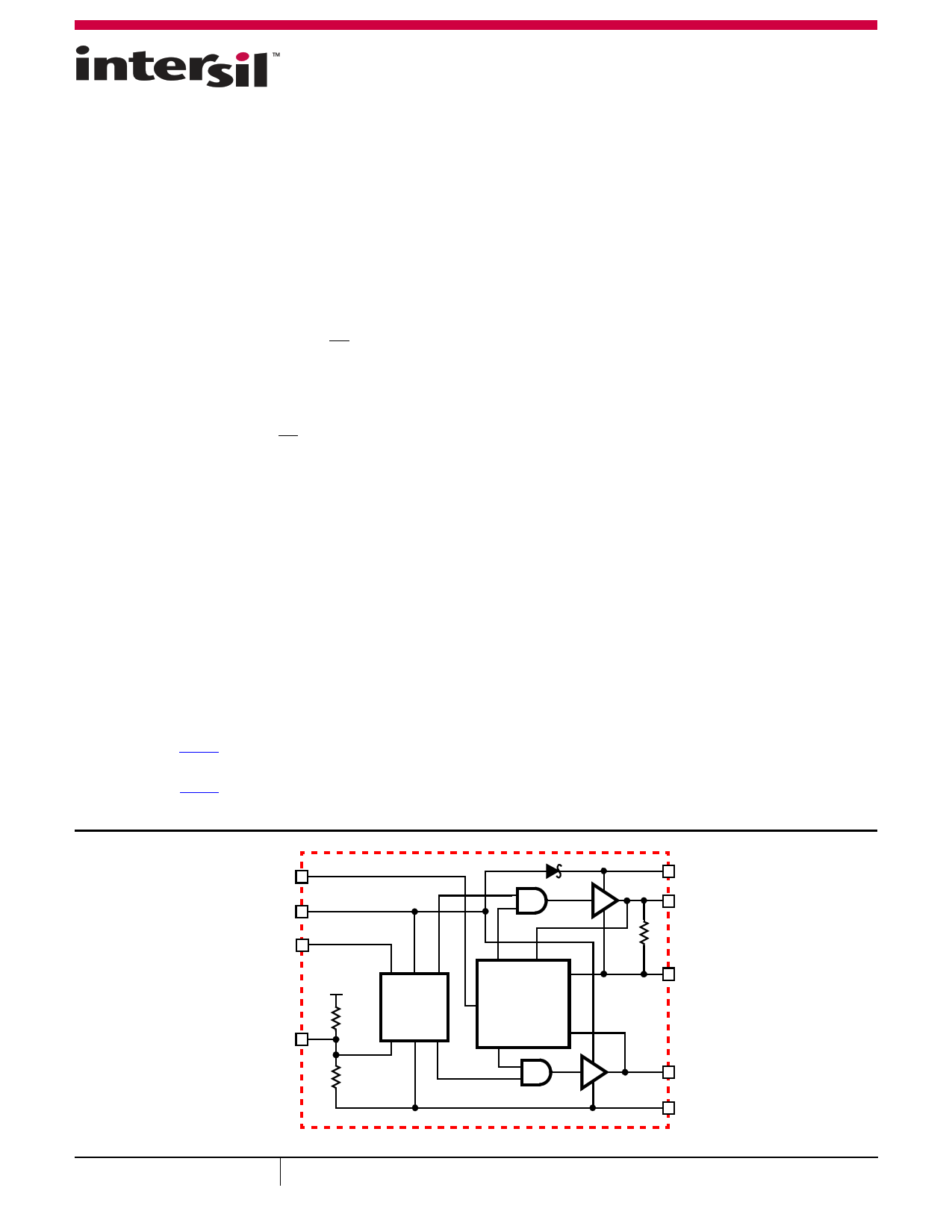
TD
VCC
EN
PWM
1
BOOT
UGATE
+5V
33.6k
POR/
CONTROL
LOGIC
SHOOT-
THROUGH
PROTECTION/
DELAY
PROGRAMMING
20kΩ
PHASE
28.8k
LGATE
GND
FIGURE 1. ISL6627 BLOCK DIAGRAM
CAUTION: These devices are sensitive to electrostatic discharge; follow proper IC Handling Procedures.
1-888-INTERSIL or 1-888-468-3774 | Copyright Intersil Americas LLC 2011, 2014. All Rights Reserved
Intersil (and design) is a trademark owned by Intersil Corporation or one of its subsidiaries.
All other trademarks mentioned are the property of their respective owners.
1 page 
ISL6627
Electrical Specifications Recommended Operating Conditions, Unless Otherwise Noted. Boldface limits apply over the operating
temperature range. (Continued)
PARAMETER
SYMBOL
TEST CONDITIONS
MIN MAX
(Note 7) TYP (Note 7) UNITS
LGATE Turn-Off Propagation Delay (Note 6)
Minimum LGATE on Time at Diode Emulation
PROPAGATION DELAY PROGRAMMING
tPDLL
tLG_ON_DM
VCC = 5V, 3nF load
VCC = 5V
14
230 330 450
ns
ns
UGATE Fall to LGATE Rise Time
tPDUFLR
VCC = 5V, 3nF Load, 90% to 10%,
short resistor from TD to VCC
23 ns
VCC = 5V, 3nF Load, 90% to 10%, 100kΩ resistor from
TD to VCC
18
ns
VCC = 5V, 3nF Load, 90% to 10%, 330kΩ resistor from
TD to VCC
15
ns
VCC = 5V, 3nF Load, 90% to 10%, 910kΩ resistor from
TD to VCC
7
ns
VCC = 5V, 3nF Load, 90% to 10%,
short resistor from TD to GND
18 ns
LGATE Fall to UGATE Rise Time
tPDLFUR
VCC = 5V, 3nF Load, 90% to 10%,
short resistor from TD to GND
40 ns
VCC = 5V, 3nF Load, 90% to 10%, 100kΩ resistor from
TD to GND
25
ns
VCC = 5V, 3nF Load, 90% to 10%, 360kΩ resistor from
TD to GND
17
ns
VCC = 5V, 3nF Load, 90% to 10%,
short resistor from TD to VCC
27 ns
OUTPUT (Note 6)
Upper Drive Source Current
I_U_SOURCE VCC = 5V, 3nF load
2A
Upper Drive Source Impedance
R_U_SOURCE 20mA source current
1Ω
Upper Drive Sink Current
I_U_SINK VCC = 5V, 3nF load
2A
Upper Drive Sink Impedance
R_U_SINK 20mA sink current
1Ω
Lower Drive Source Current
I_L_SOURCE VCC = 5V, 3nF load
2A
Lower Drive Source Impedance
R_L_SOURCE 20mA source current
1Ω
Lower Drive Sink Current
I_L_SINK VCC = 5V, 3nF load
4A
Lower Drive Sink Impedance
R_L_SINK 20mA sink current
0.4 Ω
NOTES:
6. Limits established by characterization and are not production tested.
7. Parameters with MIN and/or MAX limits are 100% tested at +25°C, unless otherwise specified. Temperature limits established by characterization
and are not production tested.
5 FN6992.1
January 24, 2014
5 Page 
ISL6627
Package Outline Drawing
L10.3x3
10 LEAD DUAL FLAT PACKAGE (DFN)
Rev 9, 10/13
3.00
A
B
5
PIN 1
INDEX AREA
5
PIN #1 INDEX AREA
1
2
(4X) 0.10
TOP VIEW
(10x 0.23)
(10 x 0.55)
10 x 0.23
0.415
0.23
0.35
0.20
1.60
BOTTOM VIEW
10x 0.35
(4X) 0.10 M C A B
SIDE VIEW
SEE DETAIL "X"
0.10 C
C
BASE PLANE
SEATING PLANE
0.08 C
(8x 0.50)
0.415
1.60
2.85 TYP
TYPICAL RECOMMENDED LAND PATTERN
C 0.20 REF
4
0.05
DETAIL "X"
NOTES:
1. Dimensions are in millimeters.
Dimensions in ( ) for Reference Only.
2. Dimensioning and tolerancing conform to ASME Y14.5m-1994.
3. Unless otherwise specified, tolerance : Decimal ± 0.05
4. Tiebar shown (if present) is a non-functional feature.
5. The configuration of the pin #1 identifier is optional, but must be
located within the zone indicated. The pin #1 identifier may be
either a mold or mark feature.
11 FN6992.1
January 24, 2014
11 Page | ||
| Páginas | Total 11 Páginas | |
| PDF Descargar | [ Datasheet ISL6627.PDF ] | |
Hoja de datos destacado
| Número de pieza | Descripción | Fabricantes |
| ISL6620 | VR11.1 Compatible Synchronous Rectified Buck MOSFET Drivers | Intersil |
| ISL6620A | VR11.1 Compatible Synchronous Rectified Buck MOSFET Drivers | Intersil |
| ISL6622 | VR11.1 Compatible Synchronous Rectified Buck MOSFET Drivers | Intersil Corporation |
| ISL6622A | VR11.1 Compatible Synchronous Rectified Buck MOSFET Drivers | Intersil Corporation |
| Número de pieza | Descripción | Fabricantes |
| SLA6805M | High Voltage 3 phase Motor Driver IC. |
Sanken |
| SDC1742 | 12- and 14-Bit Hybrid Synchro / Resolver-to-Digital Converters. |
Analog Devices |
|
DataSheet.es es una pagina web que funciona como un repositorio de manuales o hoja de datos de muchos de los productos más populares, |
| DataSheet.es | 2020 | Privacy Policy | Contacto | Buscar |