|
|
|
PDF ISL9021A Data sheet ( Hoja de datos )
| Número de pieza | ISL9021A | |
| Descripción | 250mA Single LDO | |
| Fabricantes | Intersil | |
| Logotipo | ||
Hay una vista previa y un enlace de descarga de ISL9021A (archivo pdf) en la parte inferior de esta página. Total 12 Páginas | ||
|
No Preview Available !
250mA Single LDO with Low IQ, Low Noise and High
PSRR LDO
ISL9021A
The ISL9021A is a single LDO, which provides high
performance, low input voltage and high PSRR. It delivers
guaranteed continuous 250mA load current and is stable with
1µF to 4.7µF of output capacitance (±30%) with an ESR range
of 5mΩ to 400mΩ.
The input voltage range for the ISL9021A is between 1.5V to
5.5V and the output voltage comes in many fixed voltage
options with ±1.8% accuracy over-temperature, line and load
ranges. The ISL9021A has typical PSRR of 75dB @ 10kHz and
50dB @ 1MHz.
The reverse current protection feature prevents current from
flowing back to the power source when the output voltage is
pulled higher than the input.
The ISL9021A is offered in tiny 4-bump 0.975mmx1.155mm
WLCSP and 1.6mmx1.6mm 6 Ld µTDFN packages.
Related Literature
• See FN6867, ISL9021 “250mA Single LDO with Low IQ, Low
Noise and High PSRR LDO”
Features
• High performance LDO with 250mA guaranteed continuous
output current
• Input voltage range: 1.5V to 5.5V
• Output voltage range: 1.2V to 3.3V
• High PSRR: 75dB @ 10kHz, 50dB @ 1MHz
• Low quiescent current: 35µA
• Dropout voltage: <150mV @ 250mA
• Stable with 1µF to 4.7µF output capacitance (±30%) with an
ESR range of 5mΩ to 400mΩ
• ±1.8% output accuracy over-temperature/load/line
• Soft-start limits input current surge during enable
• Current limit and overheat protection
• -40°C to +85°C operating temperature range
• Available in 0.975mmx1.155mm 4-bump WLCSP package
and 1.6mmx1.6mm 6 Ld µTDFN
• Pb-free (RoHS compliant)
Applications
• PDAs, cell phones and smart phones
• Portable instruments, MP3 players
• Handheld devices including medical handheld
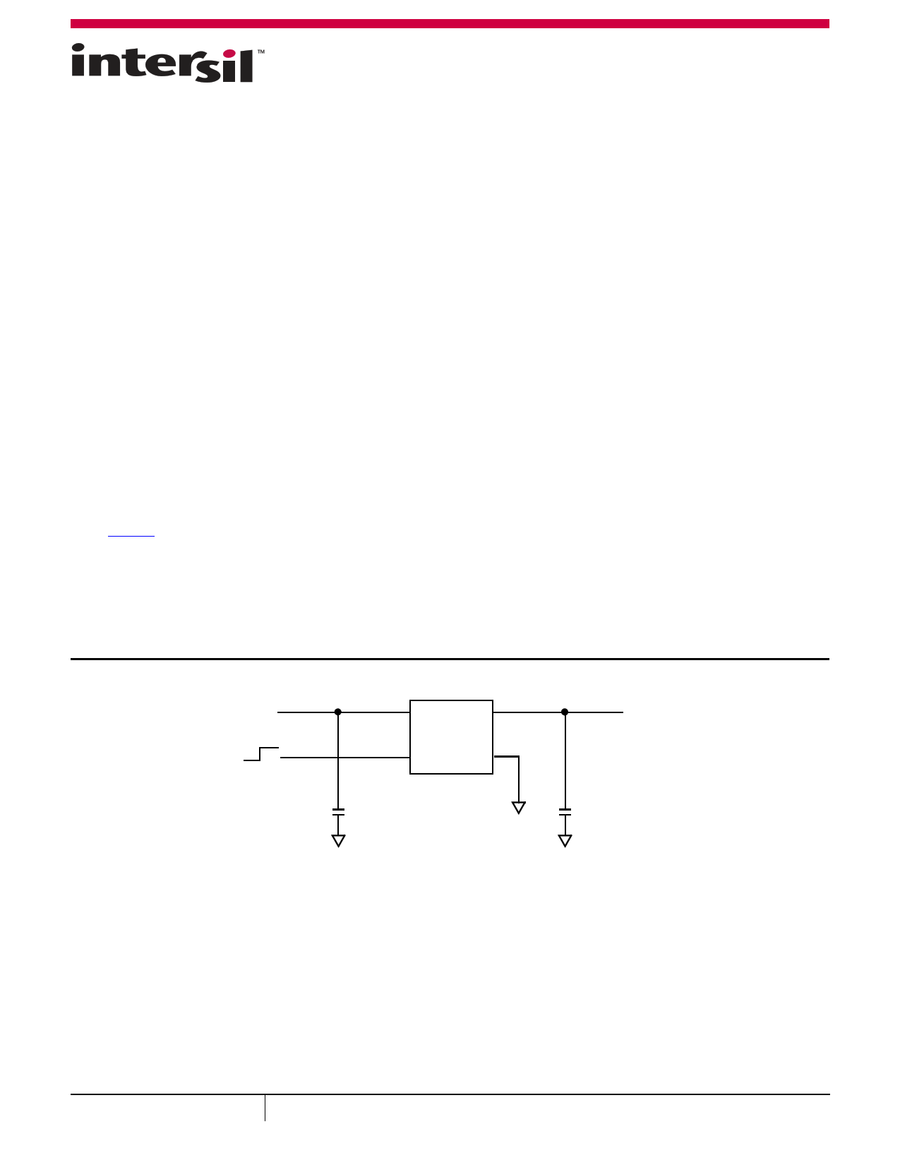
VIN (1.5V TO 5.5V)
ON
ENABLE
OFF
C1
ISL9021A
VIN VO
EN GND
C2
VOUT
FIGURE 1. TYPICAL APPLICATION
C1, C2: 1µF X5R CERAMIC CAPACITOR
December 20, 2012
FN7845.3
1
CAUTION: These devices are sensitive to electrostatic discharge; follow proper IC Handling Procedures.
1-888-INTERSIL or 1-888-468-3774 |Copyright Intersil Americas Inc. 2011, 2012. All Rights Reserved
Intersil (and design) is a trademark owned by Intersil Corporation or one of its subsidiaries.
All other trademarks mentioned are the property of their respective owners.
1 page 
ISL9021A
Absolute Maximum Ratings
Supply Voltage (VIN) . . . . . . . . . . . . . . . . . . . . . . . . . . . . . . . . . . . . . . . . +6.5V
All Other Pins . . . . . . . . . . . . . . . . . . . . . . . . . . . . . . . . . . -0.3 to (VIN + 0.3)V
Recommended Operating Conditions
Ambient Temperature Range (TA) . . . . . . . . . . . . . . . . . . . . -40°C to +85°C
Supply Voltage (VIN) . . . . . . . . . . . . . . . . . . . . . . . . . . . . . . . . . . . . 1.5 to 5.5V
ESD Rating
Human Body Model. . . . . . . . . . . . . . . . . . . . . . . . . . . . . . . . . . . . . . 5000V
Machine Model . . . . . . . . . . . . . . . . . . . . . . . . . . . . . . . . . . . . . . . . . 250V
Charged Device Model . . . . . . . . . . . . . . . . . . . . . . . . . . . . . . . . . . . 2200V
Latch-Up Passed at +85°C . . . . . . . . . . . . . . . . . . . . . . . . . . . . . . . . . 100mA
Thermal Information
Thermal Resistance (Typical)
θJA (°C/W) θJC (°C/W)
4 Ball WLCSP (Note 5) . . . . . . . . . . . . . . . . . 135.64
N/A
6 Lead µTDFN (Notes 6, 7) . . . . . . . . . . . . .
230
93
Junction Temperature Range . . . . . . . . . . . . . . . . . . . . . . .-40°C to +125°C
Operating Temperature Range . . . . . . . . . . . . . . . . . . . . . . -40°C to +85°C
Storage Temperature Range. . . . . . . . . . . . . . . . . . . . . . . .-65°C to +150°C
Pb-Free Reflow Profile . . . . . . . . . . . . . . . . . . . . . . . . . . . . . . . see link below
http://www.intersil.com/pbfree/Pb-FreeReflow.asp
CAUTION: Do not operate at or near the maximum ratings listed for extended periods of time. Exposure to such conditions may adversely impact product
reliability and result in failures not covered by warranty.
NOTES:
5. θJA is measured in free air with the component mounted on a high effective thermal conductivity test board with “direct attach” features. See Tech
Brief TB379.
6. θJA is measured with the component mounted on a high effective thermal conductivity test board in free air. See Tech Brief TB379 for details.
7. For θJC, the “case temp” location is taken at the package top center.
Electrical Specifications TA = -40°C to +85°C; VIN = (VO + 0.5V) to 5.5V with a minimum VIN of 1.5V; CIN = 1µF; CO = 1µF. Boldface
limits apply over the operating temperature range, -40°C to +85°C.
PARAMETER
SYMBOL
TEST CONDITIONS
MIN MAX
(Note 10) TYP (Note 10) UNIT
DC CHARACTERISTICS
Supply Voltage
VIN Undervoltage Lockout
Threshold
Ground Current
Shutdown Current
Output Voltage Accuracy
Maximum Output Current
Internal Current Limit
Dropout Voltage (Notes 8, 9)
Thermal Shutdown Temperature
Thermal Shutdown Hysteresis
VIN
VUVLO+
VUVLO-
IDD
IDDS
IMAX
ILIM
VDO
TSD
VIN Rising
VIN Falling
Output Enabled; IO = 0; VIN = 1.5V to 5.5V
VIN = 5.5V, EN = Low, IO = 0
VIN = VO + 0.5V to 5.5V, IO = 1mA to 250mA, TJ = +25°C
VIN = VO + 0.5V to 5.5V, IO = 1mA to 250mA, TJ = -40°C to +125°C
Continuous
IO = 250mA; VO > 1.8V
1.5
1.3
-0.8
-1.8
250
260
1.425
1.375
35
0.1
150
160
20
5.5
1.5
50
1.0
+0.8
+1.8
250
V
V
V
µA
µA
%
%
mA
mA
mV
°C
°C
AC CHARACTERISTICS
Ripple Rejection (Note 8)
Output Noise Voltage (Note 8)
DEVICE START-UP CHARACTERISTICS
VIN = 4.5V, VO = 3.3V @ 1kHz
VIN = 4.5V, VO = 3.3V @ 10kHz
VIN = 4.5V, VO = 3.3V @ 1MHz
VIN = 4.2V, TA = +25°C, BW = 10Hz to 100kHz, IO = 10mA
60
75
50
8.5*VO
dB
dB
dB
µVRMS
Device Enable Time
LDO Soft-start Ramp Rate
tEN Time from assertion of the EN pin to when the output voltage
reaches 95% of the VO (nom)
tSSR Slope of linear portion of LDO output voltage ramp during start-up
250 600
µs
30 60 µs/V
5 FN7845.3
December 20, 2012
5 Page 
ISL9021A
Package Outline Drawing
L6.1.6x1.6
6 LEAD ULTRA THIN DUAL FLAT NO-LEAD COL PLASTIC PACKAGE (UTDFN COL)
Rev 1, 11/07
1.60
6
PIN 1
INDEX AREA
A
B
PIN #1 INDEX AREA
6
1
1X 0.5 ±0.1
1.60
2X 1.00
4X 0.50
3
5X 0 . 40 ± 0 . 1
(4X) 0.15
(1.4 )
TOP VIEW
( 6X 0 . 25 )
6
BOTTOM VIEW
( 1X 0 .70 )
0 . 55 MAX
SIDE VIEW
4
0.10 M C A B
4 0.25 +0.05 / -0.07
SEE DETAIL "X"
0.10 C C
BASE PLANE
SEATING PLANE
0.08 C
( 5X 0 . 60 )
( 4X 0 . 5 )
TYPICAL RECOMMENDED LAND PATTERN
11
0 . 2 REF
C
0 . 00 MIN.
0 . 05 MAX.
DETAIL "X"
NOTES:
1. Dimensions are in millimeters.
Dimensions in ( ) for Reference Only.
2. Dimensioning and tolerancing conform to AMSE Y14.5m-1994.
3. Unless otherwise specified, tolerance : Decimal ± 0.05
4. Dimension b applies to the metallized terminal and is measured
between 0.15mm and 0.30mm from the terminal tip.
5. Tiebar shown (if present) is a non-functional feature.
6. The configuration of the pin #1 identifier is optional, but must be
located within the zone indicated. The pin #1 identifier may be
either a mold or mark feature.
FN7845.3
December 20, 2012
11 Page | ||
| Páginas | Total 12 Páginas | |
| PDF Descargar | [ Datasheet ISL9021A.PDF ] | |
Hoja de datos destacado
| Número de pieza | Descripción | Fabricantes |
| ISL9021 | Single LDO | Intersil Corporation |
| ISL9021A | 250mA Single LDO | Intersil |
| Número de pieza | Descripción | Fabricantes |
| SLA6805M | High Voltage 3 phase Motor Driver IC. |
Sanken |
| SDC1742 | 12- and 14-Bit Hybrid Synchro / Resolver-to-Digital Converters. |
Analog Devices |
|
DataSheet.es es una pagina web que funciona como un repositorio de manuales o hoja de datos de muchos de los productos más populares, |
| DataSheet.es | 2020 | Privacy Policy | Contacto | Buscar |