|
|
|
PDF SIR172ADP Data sheet ( Hoja de datos )
| Número de pieza | SIR172ADP | |
| Descripción | N-Channel 30V (D-S) MOSFET | |
| Fabricantes | Vishay | |
| Logotipo | ||
Hay una vista previa y un enlace de descarga de SIR172ADP (archivo pdf) en la parte inferior de esta página. Total 13 Páginas | ||
|
No Preview Available !
N-Channel 30 V (D-S) MOSFET
SiR172ADP
Vishay Siliconix
PRODUCT SUMMARY
VDS (V)
RDS(on) () Max.
30 0.0085 at VGS = 10 V
0.0105 at VGS = 4.5 V
ID (A)a, g
24
24
Qg (Typ.)
12.8 nC
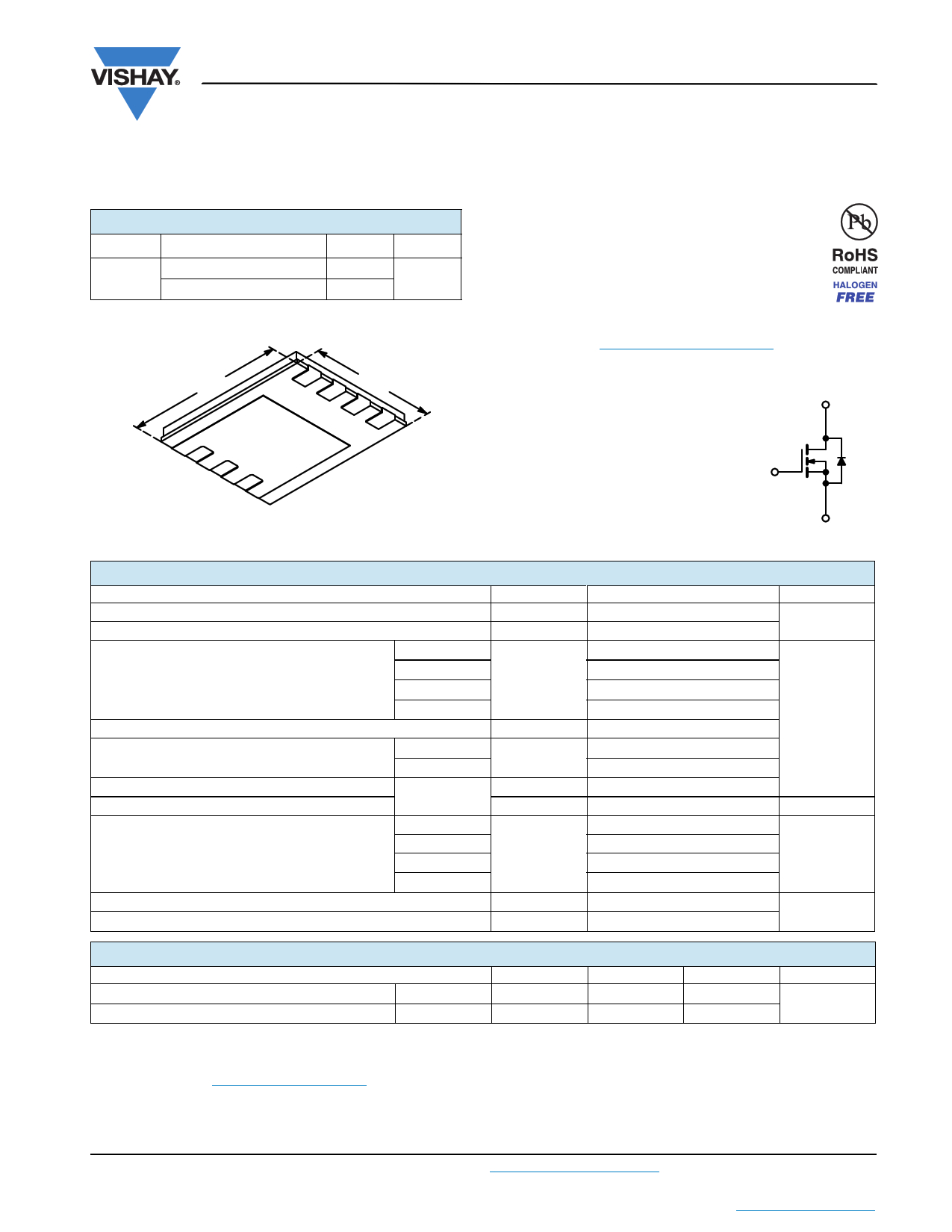
PowerPAK SO-8
FEATURES
• TrenchFET® Power MOSFET
• Low Thermal Resistance PowerPAK® Package
with Low 1.07 mm Profile
• Optimized for High-Side Synchronous Rectifier
Operation
• 100 % Rg and UIS Tested
• Material categorization: For definitions of compliance
please see www.vishay.com/doc?99912
6.15 mm
S
1S
5.15 mm
2
S
3G
4
D
8D
7
D
6
D
5
Bottom View
Ordering Information:
SiR172ADP-T1-GE3 (Lead (Pb)-free and Halogen-free)
APPLICATIONS
• Notebook CPU Core
- High-Side Switch
ABSOLUTE MAXIMUM RATINGS (TA = 25 °C, unless otherwise noted)
Parameter
Symbol
Drain-Source Voltage
VDS
Gate-Source Voltage
VGS
TC = 25 °C
Continuous Drain Current (TJ = 150 °C)
TC = 70 °C
TA = 25 °C
ID
TA = 70 °C
Pulsed Drain Current (t = 300 µs)
IDM
Continuous Source-Drain Diode Current
TC = 25 °C
TA = 25 °C
IS
Single Pulse Avalanche Current
Avalanche Energy
L = 0.1 mH
IAS
EAS
TC = 25 °C
Maximum Power Dissipation
TC = 70 °C
TA = 25 °C
PD
TA = 70 °C
Operating Junction and Storage Temperature Range
TJ, Tstg
Soldering Recommendations (Peak Temperature)d, e
Limit
30
± 20
24g
24g
16.1b, c
12.9b, c
60
24g
3.5b, c
10
5
29.8
19
3.9b, c
2.5b, c
- 55 to 150
260
D
G
S
N-Channel MOSFET
Unit
V
A
mJ
W
°C
THERMAL RESISTANCE RATINGS
Parameter
Symbol
Typical
Maximum
Unit
Maximum Junction-to-Ambientb, f
Maximum Junction-to-Case (Drain)
t 10 s
Steady State
RthJA
RthJC
27
3.5
32
°C/W
4.2
Notes:
a. Base on TC = 25 °C.
b. Surface mounted on 1" x 1" FR4 board.
c. t = 10 s.
d. See Solder Profile (www.vishay.com/doc?73257). The PowerPAK SO-8 is a leadless package. The end of the lead terminal is exposed copper
(not plated) as a result of the singulation process in manufacturing. A solder fillet at the exposed copper tip cannot be guaranteed and is not
required to ensure adequate bottom side solder interconnection.
e. Rework conditions: manual soldering with a soldering iron is not recommended for leadless components.
f. Maximum under steady state conditions is 70 °C/W.
g. Package limited.
Document Number: 62609
For technical questions, contact: [email protected]
www.vishay.com
S12-2052-Rev.B, 27-Aug-12
1
This document is subject to change without notice.
THE PRODUCTS DESCRIBED HEREIN AND THIS DOCUMENT ARE SUBJECT TO SPECIFIC DISCLAIMERS, SET FORTH AT www.vishay.com/doc?91000
1 page 
TYPICAL CHARACTERISTICS (25 °C, unless otherwise noted)
50
SiR172ADP
Vishay Siliconix
40
30
20
Limited by Package
10
0
0 25 50 75 100 125 150
TC - Case Temperature (°C)
Current Derating*
35 2.5
28 2.0
21 1.5
14 1.0
7 0.5
0
0 25 50 75 100 125 150
TC - Case Temperature (°C)
Power Derating, Junction-to-Case
0.0
0
25 50 75 100 125
TA - Ambient Temperature (°C)
Power Derating, Junction-to-Ambient
150
* The power dissipation PD is based on TJ(max.) = 150 °C, using junction-to-case thermal resistance, and is more useful in settling the upper
dissipation limit for cases where additional heatsinking is used. It is used to determine the current rating, when this rating falls below the package
limit.
Document Number: 62609
For technical questions, contact: [email protected]
www.vishay.com
S12-2052-Rev.B, 27-Aug-12
5
This document is subject to change without notice.
THE PRODUCTS DESCRIBED HEREIN AND THIS DOCUMENT ARE SUBJECT TO SPECIFIC DISCLAIMERS, SET FORTH AT www.vishay.com/doc?91000
5 Page 
www.vishay.com
Application Note AN821
Vishay Siliconix
PowerPAK® SO-8 Mounting and Thermal Considerations
SYSTEM AND ELECTRICAL IMPACT OF
PowerPAK SO-8
In any design, one must take into account the change in
MOSFET RDS(on) with temperature (figure 7).
On-Resistance vs. Junction Temperature
1.8
1.6
VGS = 10 V
ID = 23 A
1.4
1.2
1.0
0.8
0.6
- 50 - 25
0
25 50 75 100 125 150
TJ - Junction Temperature (°C)
Fig. 7 MOSFET RDS(on) vs. Temperature
A MOSFET generates internal heat due to the current
passing through the channel. This self-heating raises the
junction temperature of the device above that of the PC
board to which it is mounted, causing increased power
dissipation in the device. A major source of this problem lies
in the large values of the junction-to-foot thermal resistance
of the SO-8 package.
PowerPAK SO-8 minimizes the junction-to-board thermal
resistance to where the MOSFET die temperature is very
close to the temperature of the PC board. Consider two
devices mounted on a PC board heated to 105 °C by other
components on the board (figure 8).
Suppose each device is dissipating 2.7 W. Using the
junction-to-foot thermal resistance characteristics of the
PowerPAK SO-8 and the standard SO-8, the die
temperature is determined to be 107 °C for the PowerPAK
(and for DPAK) and 148 °C for the standard SO-8. This is a
2 °C rise above the board temperature for the PowerPAK
and a 43 °C rise for the standard SO-8. Referring to figure 7,
a 2 °C difference has minimal effect on RDS(on) whereas a
43 °C difference has a significant effect on RDS(on).
Minimizing the thermal rise above the board temperature by
using PowerPAK has not only eased the thermal design but
it has allowed the device to run cooler, keep rDS(on) low, and
permits the device to handle more current than the same
MOSFET die in the standard SO-8 package.
CONCLUSIONS
PowerPAK SO-8 has been shown to have the same thermal
performance as the DPAK package while having the same
footprint as the standard SO-8 package. The PowerPAK
SO-8 can hold larger die approximately equal in size to the
maximum that the DPAK can accommodate implying no
sacrifice in performance because of package limitations.
Recommended PowerPAK SO-8 land patterns are provided
to aid in PC board layout for designs using this new
package.
Thermal considerations have indicated that significant
advantages can be gained by using PowerPAK SO-8
devices in designs where the PC board was laid out for
the standard SO-8. Applications experimental data gave
thermal performance data showing minimum and
typical thermal performance in a SO-8 environment, plus
information on the optimum thermal performance
obtainable including spreading copper. This further
emphasized the DPAK equivalency.
PowerPAK SO-8 therefore has the desired small size
characteristics of the SO-8 combined with the attractive
thermal characteristics of the DPAK package.
PowerPAK SO-8
107 °C
Standard SO-8
148 °C
0.8 °C/W
PC Board at 105 °C
16 C/W
Fig. 8 Temperature of Devices on a PC Board
Revision: 16-Mai-13
4 Document Number: 71622
For technical questions, contact: [email protected]
THIS DOCUMENT IS SUBJECT TO CHANGE WITHOUT NOTICE. THE PRODUCTS DESCRIBED HEREIN AND THIS DOCUMENT
ARE SUBJECT TO SPECIFIC DISCLAIMERS, SET FORTH AT www.vishay.com/doc?91000
11 Page | ||
| Páginas | Total 13 Páginas | |
| PDF Descargar | [ Datasheet SIR172ADP.PDF ] | |
Hoja de datos destacado
| Número de pieza | Descripción | Fabricantes |
| SIR172ADP | N-Channel 30V (D-S) MOSFET | Vishay |
| Número de pieza | Descripción | Fabricantes |
| SLA6805M | High Voltage 3 phase Motor Driver IC. |
Sanken |
| SDC1742 | 12- and 14-Bit Hybrid Synchro / Resolver-to-Digital Converters. |
Analog Devices |
|
DataSheet.es es una pagina web que funciona como un repositorio de manuales o hoja de datos de muchos de los productos más populares, |
| DataSheet.es | 2020 | Privacy Policy | Contacto | Buscar |