|
|
|
PDF ISL33003 Data sheet ( Hoja de datos )
| Número de pieza | ISL33003 | |
| Descripción | I2C Bus Buffer | |
| Fabricantes | Intersil | |
| Logotipo | ||
Hay una vista previa y un enlace de descarga de ISL33003 (archivo pdf) en la parte inferior de esta página. Total 18 Páginas | ||
|
No Preview Available !
I2C Bus Buffer with Rise Time Accelerators and
Hot Swap Capability
ISL33001, ISL33002, ISL33003
The ISL33001, ISL33002, ISL33003 are 2-Channel Bus Buffers
that provide the buffering necessary to extend the bus
capacitance beyond the 400pF maximum specified by the I2C
specification. In addition, the ISL33001, ISL33002, ISL33003
feature rise time accelerator circuitry to reduce power
consumption from passive bus pull-up resistors and improve
data-rate performance. All devices also include hot swap circuitry
to prevent corruption of the data and clock lines when I2C devices
are plugged into a live backplane, and the ISL33002 and
ISL33003 add level translation for mixed supply voltage
applications. The ISL33001, ISL33002, ISL33003 operate at
supply voltages from +2.3V to +5.5V at a temperature range of
-40°C to +85°C.
Summary of Features
PART
NUMBER
ISL33001
ISL33002
ISL33003
LEVEL
TRANSLATION
No
Yes
Yes
ENABLE
PIN
Yes
No
Yes
READY
PIN
Yes
No
No
ACCELERATOR
DISABLE
No
Yes
No
Related Literature
• AN1543, “ISL33001MSOPEVAL1Z, ISL33002MSOPEVAL1Z,
ISL33003MSOPEVAL1Z Evaluation Board User’s Manual”
• AN1637, “Level Shifting Between 1.8V and 3.3V Using I2C
Buffers”
Features
• 2 Channel I2C compatible bi-directional buffer
• +2.3VDC to +5.5VDC supply range
• >400kHz operation
• Bus capacitance buffering
• Rise time accelerators
• Hot swapping capability
• ±6kV Class 3 HBM ESD protection on all pins
• ±12kV HBM ESD protection on SDA/SCL pins
• Enable pin (ISL33001 and ISL33003)
• Logic level translation (ISL33002 and ISL33003)
• READY logic pin (ISL33001)
• Accelerator disable pin (ISL33002)
• Pb-free (RoHS Compliant) 8 Ld SOIC (ISL33001 only),
8 Ld TDFN (3mmx3mm) and 8 Ld MSOP packages
• Low quiescent current . . . . . . . . . . . . . . . . . . . . . . . 2.1mA typ
• Low shutdown current . . . . . . . . . . . . . . . . . . . . . . . . 0.5µA typ
Applications
• I2C bus extender and capacitance buffering
• Server racks for telecom, datacom, and computer servers
• Desktop computers
• Hot-swap board insertion and bus isolation
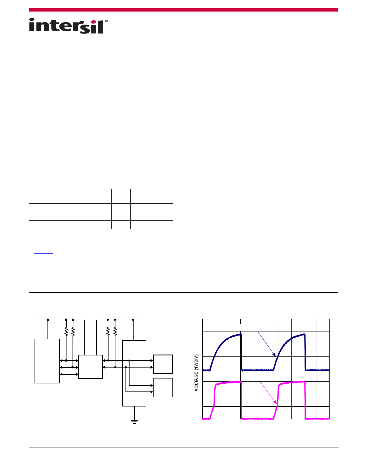
VCC1 +3.3V
+5.0V
VCC2
µC
SDA
SCL
EN
ISL33003
BACK
PLANE
SDA
SCL
GND
I2C
DEVICE
A
I2C
DEVICE
B
100kHz I2C BUS WITH 2.7kΩ PULL-UP RESISTOR
AND 400pF BUS CAPACITANCE
WITHOUT BUFFER
WITH BUFFER
FIGURE 1. TYPICAL OPERATING CIRCUIT
TIME (2µs/DIV)
FIGURE 2. BUS ACCELERATOR PERFORMANCE
July 11, 2014
FN7560.6
1
CAUTION: These devices are sensitive to electrostatic discharge; follow proper IC Handling Procedures.
1-888-INTERSIL or 1-888-468-3774 |Copyright Intersil Americas LLC. 2010-2014. All Rights Reserved
Intersil (and design) is a trademark owned by Intersil Corporation or one of its subsidiaries.
All other trademarks mentioned are the property of their respective owners.
1 page 
ISL33001, ISL33002, ISL33003
Electrical Specifications VEN = VCC1, VCC1 = +2.3V to +5.5V, VCC2 = +2.3V to +5.5V, unless otherwise noted (Note 8). Boldface limits apply
over the operating temperature range, -40°C to +85°C. (Continued)
PARAMETER
SYMBOL
CONDITIONS
TEMP
MIN
MAX
(°C) (Note 9) TYP (Note 9) UNITS
Ready Delay, Off-On
Ready Output Low Voltage
RISE-TIME ACCELERATORS
tREADY-LH
VOL_READY
ISL33001 only (Note 10)
VCC1 = +2.5V, IPULLUP = 3mA; ISL33001 only
+25
Full
-
-
10 - ns
- 0.4 V
Transient Accelerator
ITRAN_ACC VCC1 = 2.7V, VCC2 = 2.7V ; (ACC = 0.7*VCC1 for +25
-
5
- mA
Current
ISL33002 only) (Figure 8)
Accelerator Pin Enable
Threshold
VACC_EN ISL33002 only
+25
-
0.5*VCC1 0.7*VCC1
V
Accelerator Pin Disable
Threshold
VACC_DIS ISL33002 only
+25 0.3*VCC1 0.5*VCC1
-
V
Accelerator Pin Input
Current
IACC ISL33002 only
+25 -1 0.1 1 µA
Accelerator Delay, On-Off
ESD PROTECTION
tPDOFF ISL33002 only (Note 10)
+25 - 10 - ns
SDA, SCL I/O Pins
Human Body Model, SDA and SCL pins to ground +25
-
±12
- kV
only (JESD22-A114)
All Pins
Machine Model (JESD22-A115)
+25 -
±400
-
V
Class 3 HBM ESD (JESD22-A114)
+25
±6 - kV
INPUT-OUTPUT CONNECTIONS
Input Low Threshold
Input-Output Offset
Voltage
VIL VCC1 = VCC2, 10kto VCC1 on SDA and SCL pins +25
VOS VCC1 = 3.3V, 10kto VCC1 on SDA and SCL pins, Full
VINPUT = 0.2V; VCC2 = 3.3V, ISL33002 and
ISL33003 (Figure 5)
-
0
-
0.3*VCC1
V
50 150 mV
Output Low Voltage
VOL VCC1 = 2.7V, VINPUT = 0V, ISINK = 3mA on
Full -
SDA/SCL pins; VCC2 = 2.7V, ISL33002 and
ISL33003 (Figure 6)
- 0.4 V
Buffer SDA and SCL Pins
Input Capacitance
CIN (Figure 25)
+25 - 10 - pF
Input Leakage Current
TIMING CHARACTERISTICS
ILEAK
SDA and SCL pins = VCC1 = 5.5V;
VCC2 = 5.5V, ISL33002 and ISL33003
Full -5 0.1 5 µA
SCL/SDA Propagation
Delay High-to-Low
tPHL CLOAD = 100pF, 2.7kto VCC1 on SDA and SCL +25
pins, VCC1 = 3.3V; VCC2 = 3.3V, ISL33002 and
ISL33003 (Figure 7)
0
27 100 ns
SCL/SDA Propagation
Delay Low-to-High
tPLH CLOAD = 100pF, 2.7kto VCC1 on SDA and SCL +25
pins, VCC1 = 3.3V; VCC2 = 3.3V, ISL33002 and
ISL33003 (Figure 7)
0
2 26 ns
NOTES:
8. The algebraic convention, whereby the most negative value is a minimum and the most positive a maximum, is used in this data sheet.
9. Parameters with MIN and/or MAX limits are 100% tested at +25°C, unless otherwise specified. Temperature limits established by characterization
and are not production tested.
10. Typical value determined by design simulations. Parameter not tested.
11. Buffer is in the connected state.
12. ISL33002 and ISL33003 limits established by characterization. Not production tested.
13. If the VCC1 and VCC2 voltages diverge, then the shut down ICC increases on the higher voltage supply.
Submit Document Feedback
5
FN7560.6
July 11, 2014
5 Page 
ISL33001, ISL33002, ISL33003
Typical Performance Curves CIN = COUT = 10pF, VCC1 = VCC2 = VCC, TA = +25°C; Unless Otherwise Specified.
2.4
2.3 T = -40°C
2.2
2.1 T = +25°C
2.0 T = +85°C
1.9
1.8
1.7
1.6
1.5
1.4
1.3
1.2
2.0 2.5 3.0 3.5 4.0 4.5 5.0 5.5 6.0
VCC1 (V)
600
550
500
450 T = +25°C
400 T = +85°C
350
300
250
200
150
100
2.0 2.5 3.0 3.5 4.0 4.5 5.0 5.5 6.0
VCC1 (V)
FIGURE 11. ICC1 ENABLED CURRENT vs VCC1 (ISL33001)
FIGURE 12. ICC1 DISABLED CURRENT vs VCC1 (ISL33001)
2.4
2.3 VCC2 = 5.5V
2.2
2.1 T = +85°C
2.0
1.9
T = -40°C
T = +25°C
1.8
1.7
1.6
1.5
1.4
1.3
1.2
2.0 2.5 3.0 3.5 4.0 4.5 5.0 5.5 6.0
VCC1 (V)
FIGURE 13. ICC1 ENABLED CURRENT vs VCC1 (ISL33002 AND
ISL33003)
0.24
0.22
0.20
0.18
VCC1 = 5.5V
T = +85°C
T = -40°C
T = +25°C
0.16
0.14
0.12
0.10
2.0 2.5 3.0 3.5 4.0 4.5 5.0 5.5 6.0
VCC2 (V)
FIGURE 15. ICC2 ENABLED CURRENT vs VCC2 (ISL33002 AND
ISL33003)
60
VCC2 = 5.5V
50
40
30 T = +25°C
T = +85°C
20
10
0
2.0 2.5 3.0 3.5 4.0 4.5 5.0 5.5 6.0
VCC1 (V)
FIGURE 14. ICC1 DISABLED CURRENT vs VCC1 (ISL33003)
60
VCC1 = 5.5V
50
40
30
T = +85°C
T = +25°C
20
10
0
2.0 2.5 3.0 3.5 4.0 4.5 5.0 5.5 6.0
VCC2 (V)
FIGURE 16. ICC2 DISABLED CURRENT vs VCC2 (ISL33003)
Submit Document Feedback 11
FN7560.6
July 11, 2014
11 Page | ||
| Páginas | Total 18 Páginas | |
| PDF Descargar | [ Datasheet ISL33003.PDF ] | |
Hoja de datos destacado
| Número de pieza | Descripción | Fabricantes |
| ISL33001 | I2C Bus Buffer | Intersil |
| ISL33002 | I2C Bus Buffer | Intersil |
| ISL33003 | I2C Bus Buffer | Intersil |
| Número de pieza | Descripción | Fabricantes |
| SLA6805M | High Voltage 3 phase Motor Driver IC. |
Sanken |
| SDC1742 | 12- and 14-Bit Hybrid Synchro / Resolver-to-Digital Converters. |
Analog Devices |
|
DataSheet.es es una pagina web que funciona como un repositorio de manuales o hoja de datos de muchos de los productos más populares, |
| DataSheet.es | 2020 | Privacy Policy | Contacto | Buscar |