|
|
PDF N01S818HA Data sheet ( Hoja de datos )
| Número de pieza | N01S818HA | |
| Descripción | 1 Mb Ultra-Low Power Serial SRAM | |
| Fabricantes | ON Semiconductor | |
| Logotipo | ||
Hay una vista previa y un enlace de descarga de N01S818HA (archivo pdf) en la parte inferior de esta página. Total 12 Páginas | ||
|
No Preview Available !
N01S818HA
1 Mb Ultra-Low Power
Serial SRAM
Standard SPI Interface and Multiplex
DUAL and QUAD Interface
Overview
The ON Semiconductor serial SRAM family includes several
integrated memory devices including this 1 Mb serially accessed
Static Random Access Memory, internally organized as 128 K words
by 8 bits. The devices are designed and fabricated using
ON Semiconductor’s advanced CMOS technology to provide both
high-speed performance and low power. The devices operate with a
single chip select (CS) input and use a simple Serial Peripheral
Interface (SPI) protocol. In SPI mode, a single data-in (SI) and
data-out (SO) line is used along with the clock (SCK) to access data
within the device. In DUAL mode, two multiplexed data-in/data-out
(SIO0-SIO1) lines are used and in QUAD mode, four multiplexed
data-in/data-out (SIO0-SIO3) lines are used with the clock to access
the memory.
The devices can operate over a wide temperature range of −40°C to
+85°C and are available in a 8-lead TSSOP package.
Features
• Power Supply Range: 1.7 to 2.2 V
• Very Low Typical Standby Current < 1 mA
• Very Low Operating Current < 10 mA
• Simple Serial Interface
♦ Single-bit SPI Access
♦ DUAL-bit and QUAD-bit SPI-like Access
• Flexible Operating Modes
♦ Word Mode
♦ Page Mode
♦ Burst Mode (Full Array)
• High Frequency Read and Write Operation
♦ Clock Frequency 20 MHz
• Built-in Write Protection (CS High)
• High Reliability
♦ Unlimited Write Cycles
• These Devices are Pb−Free and are RoHS Compliant
♦ Green TSSOP
http://onsemi.com
TSSOP8 3x4.4
CASE 948BH
PACKAGE CONFIGURATION
CS
SO / SIO1
NC / SIO2
VSS
1
2
3
4
8 VCC
7 HOLD / SIO3
6 SCK
5 SI / SIO0
ORDERING INFORMATION
Device
Package
Shipping†
N01S818HAT22I TSSOP−8
(Pb−Free)
N01S818HAT22IT TSSOP−8
(Pb−Free)
100 Units / Tube
3000 / Tape & Reel
†For information on tape and reel specifications,
including part orientation and tape sizes, please
refer to our Tape and Reel Packaging Specification
Brochure, BRD8011/D.
Table 1. DEVICE OPTIONS
Device / Part Number
N01S818HAT22I
Power Supply
1.7 V − 2.2 V
© Semiconductor Components Industries, LLC, 2013
September, 2013 − Rev. 0
Speed
20 MHz
1
Package
TSSOP−8
Function
HOLD
Publication Order Number:
N01S818HA/D
1 page 
N01S818HA
Write Operation
The serial SRAM WRITE is selected by enabling CS low.
First, the 8-bit WRITE instruction is transmitted to the
device followed by the 24-bit address with the 7 MSBs being
don’t care. After the WRITE instruction and addresses are
sent, the data to be stored in memory is shifted in on the SI
pin.
If operating in page mode, after the initial word of data is
shifted in, additional data words can be written as long as the
address requested is sequential on the same page. Simply
write the data on SI pin and continue to provide clock pulses.
The internal address pointer is automatically incremented to
the next higher address on the page after each word of data
is written in. This can be continued for the entire page length
of 32 words long. At the end of the page, the addresses
pointer will be wrapped to the 0 word address within the
page and the operation can be continuously looped over the
32 words of the same page. The new data will replace data
already stored in the memory locations.
If operating in burst mode, after the initial word of data is
shifted in, additional data words can be written to the next
sequential memory locations by continuing to provide clock
pulses. The internal address pointer is automatically
incremented to the next higher address after each word of
data is read out. This can be continued for the entire array
and when the highest address is reached, 1FFFFh, the
address counter wraps to the address 00000h. This allows
the burst write cycle to be continued indefinitely. Again, the
new data will replace data already stored in the memory
locations.
All WRITE operations are terminated by pulling CS high.
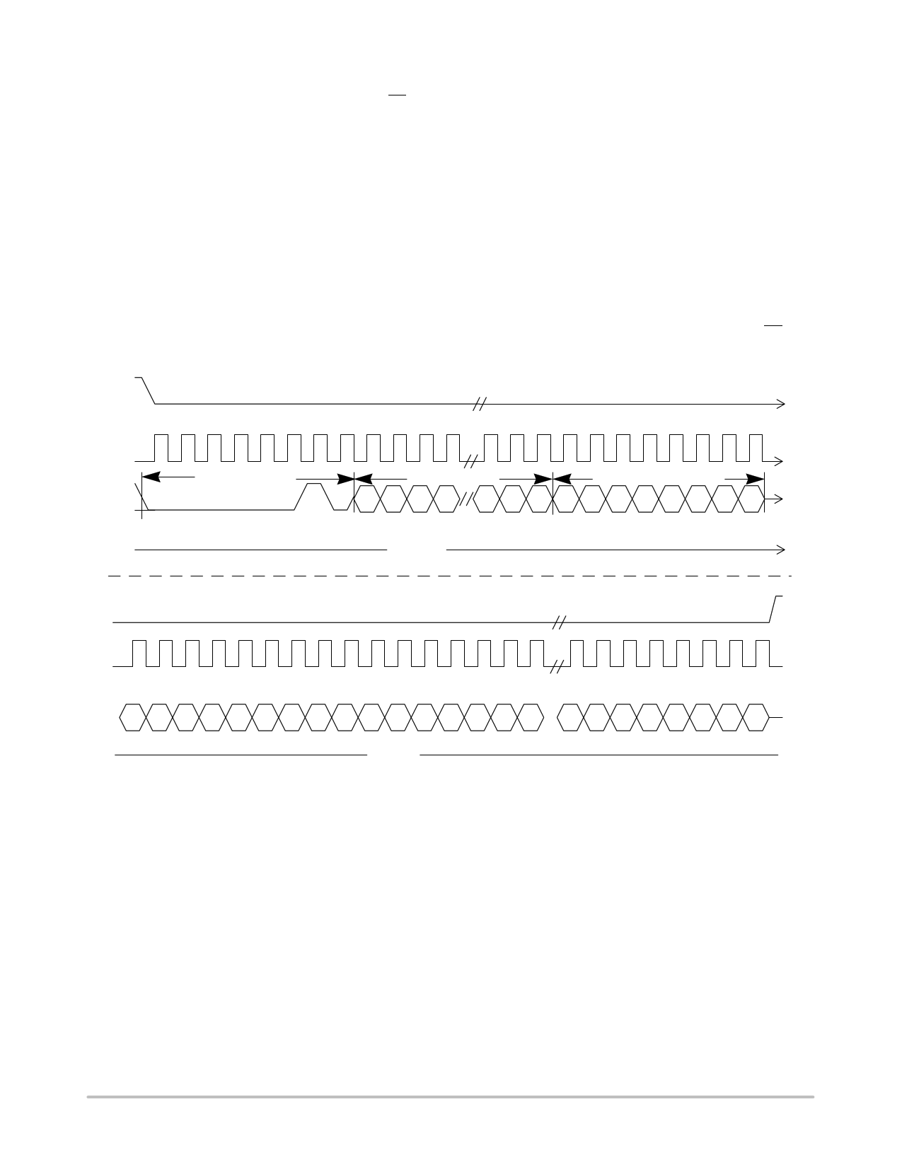
CS
SCK 0 1 2 3 4 5 6 7 8 9 10 11
29 30 31 32 33 34 35 36 37 38 39
Instruction
24−bit address
Data In to ADDR 1
SI 0 0 0 0 0 0 1 0 23 22 21 20
21076543210
ADDR 1
SO High−Z
40 41 42 43 44 45 46 47 48 49 50 51 52 53 54 55
Data In to ADDR 2
Data In to ADDR 3
Data In to ADDR n
7 6 5 4 3 2 1 0 7 6 5 4 3 2 1 0 ... 7 6 5 4 3 2 1 0
High−Z
Figure 6. SPI Write Sequence
http://onsemi.com
5
5 Page 
N01S818HA
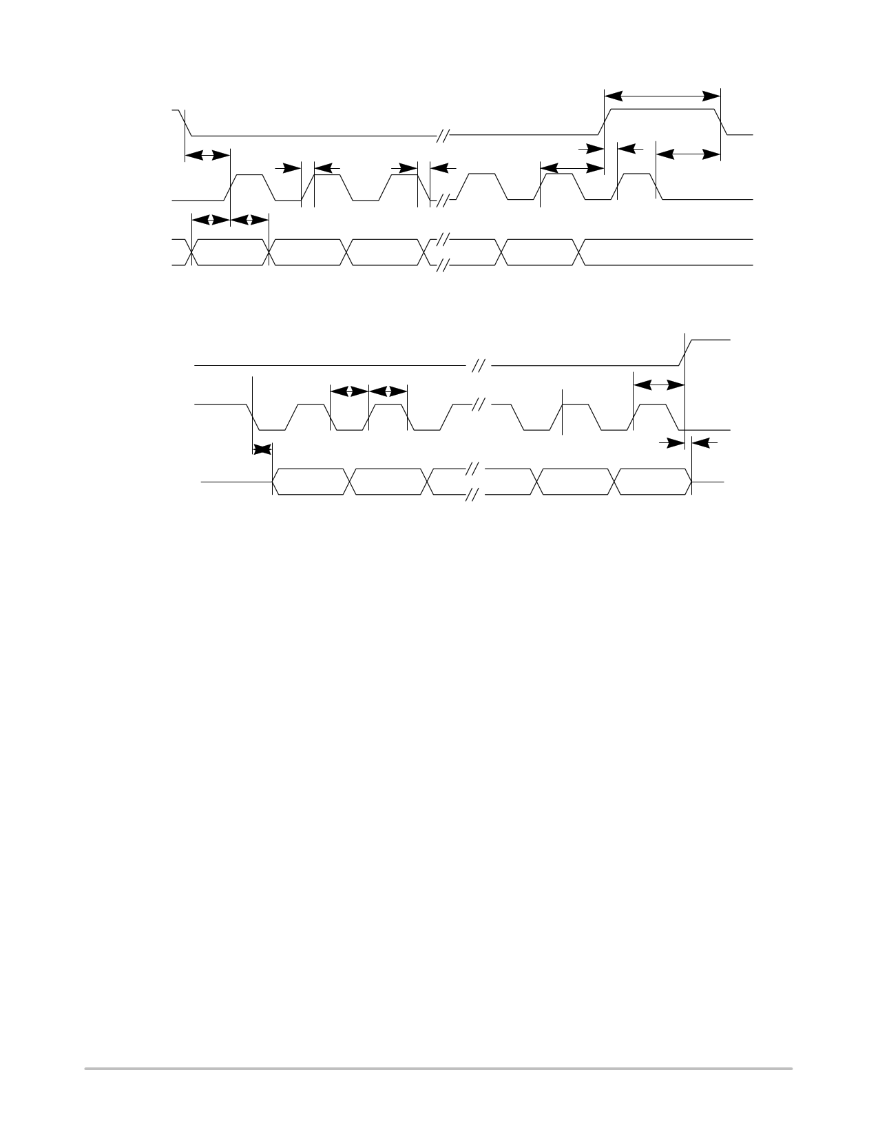
CS
SCK
tCSS
tSU
SI0 MSB in
tR
tHD
tF tCSH
LSB in
Figure 18. QUAD Input Timing
tCSD
tCLD
tSCS
CS
SCK
SIO
tLO tHI
tV
MSB out
Figure 19. QUAD Output Timing
tCSH
LSB out
tDIS
http://onsemi.com
11
11 Page | ||
| Páginas | Total 12 Páginas | |
| PDF Descargar | [ Datasheet N01S818HA.PDF ] | |
Hoja de datos destacado
| Número de pieza | Descripción | Fabricantes |
| N01S818HA | 1 Mb Ultra-Low Power Serial SRAM | ON Semiconductor |
| Número de pieza | Descripción | Fabricantes |
| SLA6805M | High Voltage 3 phase Motor Driver IC. |
Sanken |
| SDC1742 | 12- and 14-Bit Hybrid Synchro / Resolver-to-Digital Converters. |
Analog Devices |
|
DataSheet.es es una pagina web que funciona como un repositorio de manuales o hoja de datos de muchos de los productos más populares, |
| DataSheet.es | 2020 | Privacy Policy | Contacto | Buscar |
