|
|
|
PDF STP13N80K5 Data sheet ( Hoja de datos )
| Número de pieza | STP13N80K5 | |
| Descripción | N-channel Power MOSFET | |
| Fabricantes | STMicroelectronics | |
| Logotipo | ||
Hay una vista previa y un enlace de descarga de STP13N80K5 (archivo pdf) en la parte inferior de esta página. Total 24 Páginas | ||
|
No Preview Available !
STB13N80K5, STF13N80K5,
STP13N80K5, STW13N80K5
N-channel 800 V, 0.37 Ω typ., 12 A SuperMESH™ 5 Power
MOSFETs in D²PAK, TO-220FP, TO-220 and TO-247 packages
Datasheet - production data
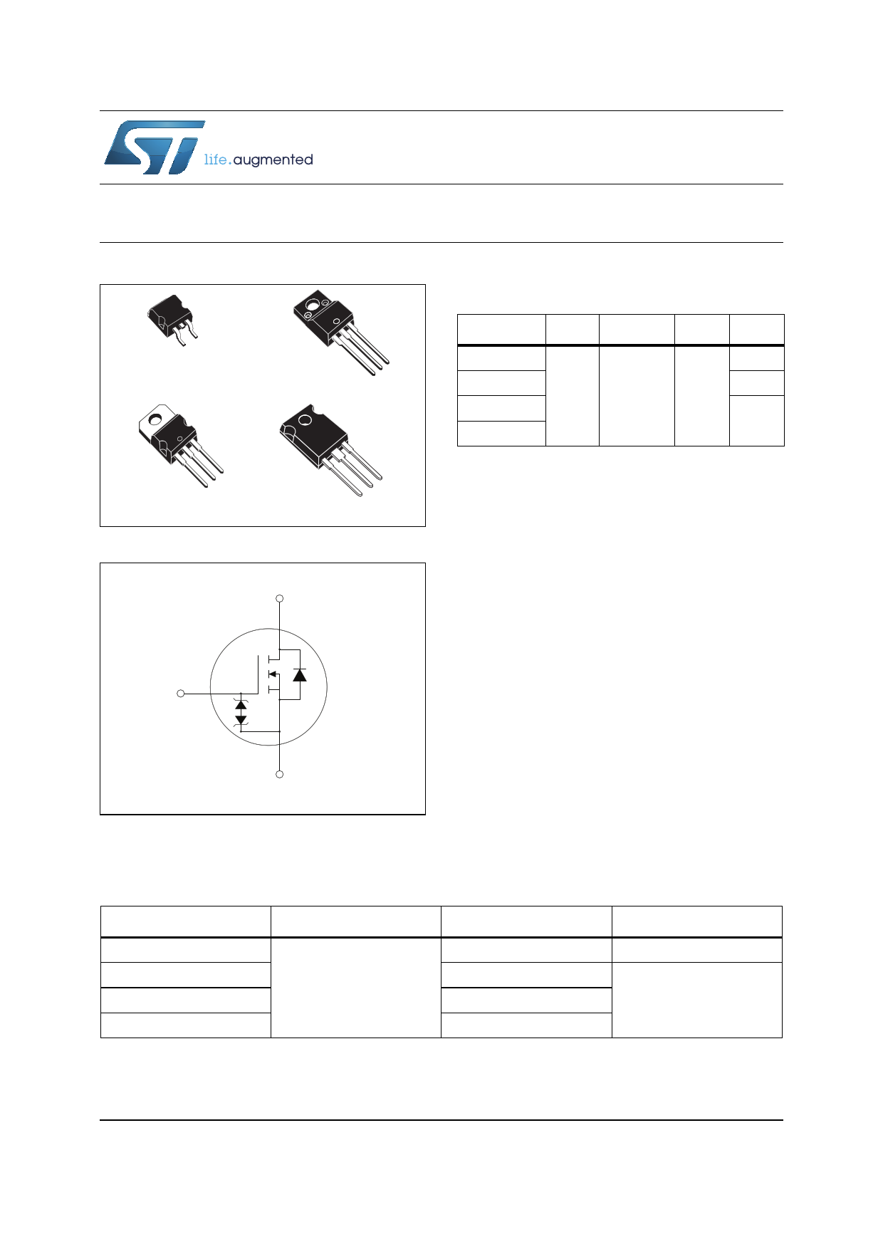
TAB
3
1
D2PAK
TAB
3
2
1
TO-220FP
3
2
1
TO-220
3
2
1
TO-247
Figure 1. Internal schematic diagram
D(2, TAB)
Features
Order codes VDS
RDS(on)
ID PTOT
STB13N80K5
190 W
STF13N80K5
800 V
STP13N80K5
STW13N80K5
0.45 Ω
12 A
35 W
190 W
• Worldwide best FOM (figure of merit)
• Ultra low gate charge
• 100% avalanche tested
• Zener-protected
Applications
• Switching applications
G(1)
S(3)
AM01476v1
Description
These devices are N-channel Zener-protected
Power MOSFETs realized in SuperMESH™ 5, a
revolutionary avalanche-rugged very high voltage
Power MOSFET technology based on an
innovative proprietary vertical structure. The
result is a drastic reduction in on-resistance and
ultra low gate charge for applications which
require superior power density and high
efficiency.
Order codes
STB13N80K5
STF13N80K5
STP13N80K5
STW13N80K5
Table 1. Device summary
Marking
Packages
13N80K5
D²PAK
TO-220FP
TO-220
TO-247
Packaging
Tape and reel
Tube
June 2014
This is information on a product in full production.
DocID024348 Rev 4
1/24
www.st.com
24
1 page 
STB13N80K5, STF13N80K5, STP13N80K5, STW13N80K5
Electrical characteristics
Symbol
Table 6. Switching times
Parameter
Test conditions
td(on)
tr
td(off)
tf
Turn-on delay time
Rise time
Turn-off delay time
Fall time
VDD = 400 V, ID = 6A,
RG=4.7 Ω, VGS=10 V
(see Figure 24)
Min. Typ. Max. Unit
- 16 - ns
- 16 - ns
- 42 - ns
- 16 - ns
Symbol
Table 7. Source drain diode
Parameter
Test conditions
ISD Source-drain current
ISDM Source-drain current (pulsed)
(1)
VSD Forward on voltage
VGS=0, ISD= 12 A
trr
Qrr
IRRM
Reverse recovery time
Reverse recovery charge
Reverse recovery current
ISD= 12 A, VDD= 60 V
di/dt = 100 A/μs,
(see Figure 23)
trr
Qrr
IRRM
Reverse recovery time
Reverse recovery charge
Reverse recovery current
ISD= 12 A,VDD= 60 V
di/dt=100 A/μs,
Tj=150 °C
(see Figure 23)
1. Pulsed: pulse duration = 300μs, duty cycle 1.5%
Min. Typ. Max. Unit
- 14 A
- 56 A
- 1.5 V
- 406
ns
- 5.7
μC
- 28
A
- 600
ns
- 7.9
μC
- 26
A
Symbol
Table 8. Gate-source Zener diode
Parameter
Test conditions
Min. Typ. Max Unit
V(BR)GSO Gate-source breakdown voltage IGS= ± 1mA, ID= 0
30 - - V
The built-in back-to-back Zener diodes have specifically been designed to enhance the
device's ESD capability. In this respect the Zener voltage is appropriate to achieve an
efficient and cost-effective intervention to protect the device's integrity. These integrated
Zener diodes thus avoid the usage of external components.
DocID024348 Rev 4
5/24
5 Page 
STB13N80K5, STF13N80K5, STP13N80K5, STW13N80K5
4 Package mechanical data
Package mechanical data
In order to meet environmental requirements, ST offers these devices in different grades of
®®
ECOPACK packages, depending on their level of environmental compliance. ECOPACK
specifications, grade definitions and product status are available at: www.st.com.
®
ECOPACK is an ST trademark.
DocID024348 Rev 4
11/24
11 Page | ||
| Páginas | Total 24 Páginas | |
| PDF Descargar | [ Datasheet STP13N80K5.PDF ] | |
Hoja de datos destacado
| Número de pieza | Descripción | Fabricantes |
| STP13N80K5 | N-channel Power MOSFET | STMicroelectronics |
| Número de pieza | Descripción | Fabricantes |
| SLA6805M | High Voltage 3 phase Motor Driver IC. |
Sanken |
| SDC1742 | 12- and 14-Bit Hybrid Synchro / Resolver-to-Digital Converters. |
Analog Devices |
|
DataSheet.es es una pagina web que funciona como un repositorio de manuales o hoja de datos de muchos de los productos más populares, |
| DataSheet.es | 2020 | Privacy Policy | Contacto | Buscar |