|
|
|
PDF 74LVC244A Data sheet ( Hoja de datos )
| Número de pieza | 74LVC244A | |
| Descripción | OCTAL BUFFER/LINE DRIVER | |
| Fabricantes | Diodes | |
| Logotipo | ||
Hay una vista previa y un enlace de descarga de 74LVC244A (archivo pdf) en la parte inferior de esta página. Total 10 Páginas | ||
|
No Preview Available !
74LVC244A
OCTAL BUFFER/LINE DRIVER WITH 3 STATE OUTPUTS
Description
The 74LVC244A provides two 4-bit line drivers with separate output-
enable (OE) inputs. When OE is low, the device passes data from the
A inputs to the Y outputs. When OE is high, the outputs are in the
high-impedance state.
The device is designed for operation with a power supply range of
1.65V to 3.6V.
The inputs are tolerant to 5.5V allowing this device to be used in a
mixed voltage environment. The device is fully specified for partial
power down applications using IOFF. The IOFF circuitry disables the
output preventing damaging current backflow when the device is
powered down.
Features
• Supply Voltage Range from 1.65V to 3.6V
• Sinks or Sources 24ma at VCC = 3V
• CMOS Low Power Consumption
• IOFF Supports Partial - Power Down Operation
• Inputs or Outputs Accept up to 5.5V
• Inputs can be Driven by 3.3V or 5V Allowing for Mixed Voltage
Applications
• Schmitt Trigger Action at All Inputs
• Typical VOLP (Quiet Output Ground Bounce) Less than 0.8V with
VCC = 3.3V and TA = +25°C
• Typical VOHV (Quiet Output Dynamic VOH) Greater than 2.0V
with VCC = 3.3V and TA = +25°C
• ESD Protection Tested per JESD 22
Exceeds 200-V Machine Model (A115)
Exceeds 2000-V Human Body Model (A114)
Exceeds 1000-V Charged Device Model (C101)
• Latch-Up Exceeds 250mA per JESD 78, Class I
• All devices are:
Totally Lead-Free & Fully RoHS compliant (Notes 1 & 2)
Halogen and Antimony Free. “Green” Device (Note 3)
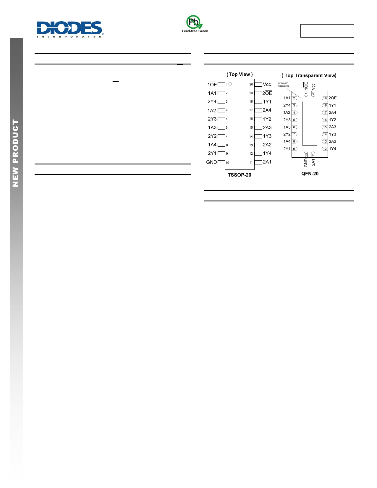
Pin Assignments
Applications
• General Purpose Logic
• Bus Driving
• Power Down Signal Isolation
• Wide array of products such as:
PCs, Notebooks, Netbooks, Ultrabooks
Networking Computer Peripherals, Hard Drives, CD/DVD
ROM
TV, DVD, DVR, Set Top Box
Notes:
1. No purposely added lead. Fully EU Directive 2002/95/EC (RoHS) & 2011/65/EU (RoHS 2) compliant.
2. See http://www.diodes.com/quality/lead_free.html for more information about Diodes Incorporated’s definitions of Halogen and Antimony free,
"Green" and Lead-Free.
3. Halogen and Antimony free "Green” products are defined as those which contain <900ppm bromine, <900ppm chlorine (<1500ppm total Br + Cl) and
<1000ppm antimony compounds.
74LVC244A
Document number: DS35888 Rev. 1 - 2
1 of 10
www.diodes.com
July 2014
© Diodes Incorporated
1 page 
74LVC244A
Switching Characteristics
Symbol
Parameter
Test
Conditions
Propagation
tPD Delay AN to YN Figure 1
Enable Time
tEN
OE to YN
Figure 1
tDIS
tsk(0)
Disable Time
OE to YN
Figure 1
Output Skew
Time
VCC
1.5V
1.8V ± 0.15V
2.5V ± 0.2V
2.7V
3.3V ± 0.3
1.5V
1.8V ± 0.15V
2.5V ± 0.2V
2.7V
3.3V ± 0.3
1.5V
1.8V ± 0.15V
2.5V ± 0.2V
2.7V
3.3V ± 0.3
3.3V ± 0.3
TA = +25°C
Min Typ Max
1 7 16.9
1 6.0 11.4
1 3.9 7.4
1 4.2 7.7
1.5 3.8 7.3
1 12.4 18.3
1 6.4 12.1
1 4.6 9.1
1 5 8.4
1.5 4.5 7.4
1 7.2 15.6
1 5.8 11.6
1 3.7 7.3
1 3.8 6.6
1.5 3.8 6.3
— — 1.0
TA = -40° to
+85°C
Min Max
1 18.9
1 11.3
1 8.0
1 8.5
1.5 7.7
1 19.8
1 12.6
1 9.6
1 8.6
1.5 7.6
1 16.1
1 12.1
1 7.8
1 6.8
1.5 6.5
——
TA = -40° to
+125°C
Min Max
1 20.4
1 12.4
1 10.0
1 8.8
1.5 7.9
1 25.4
1 14.1
1 11.7
1 10.3
1.5 9.4
1 17.6
1 13.6
1 9.9
1 8.6
1.5 8
— 1.5
Unit
ns
ns
ns
ns
Operating Characteristics
TA = +25°C
Symbol
Parameter
Test Conditions
Cpd
Power dissipation
F= 10 MHz
capacitance per gate Outputs Enabled
VCC
1.8V± 0.15V
2.5V± 0.2V
3.3V± 0.3V
Typ
9.9
10.2
10.6
Unit
pF
Package Characteristics
Symbol
θJA
θJC
θJA
θJC
Parameter
Thermal Resistance
Junction-to-Ambient
Thermal Resistance
Junction-to-Case
Thermal Resistance
Junction-to-Ambient
Thermal Resistance
Junction-to-Case
Package
TSSOP-20
Test Conditions
Min
Typ
Max Unit
(Note 9)
— 74 — °C/W
TSSOP-20
(Note 9)
— 15 — °C/W
V-QFN4525-20
(Note 9)
— 67 — °C/W
V-QFN4525-20
(Note 9)
— 20 — °C/W
Note:
9. Test conditions for TSSOP-20 and V-QFN4525-20: Devices mounted on 4 layer FR-4 substrate PC board, 2oz copper, with minimum recommended
pad layout per JESD 51-7.
74LVC244A
Document number: DS35888 Rev. 1 - 2
5 of 10
www.diodes.com
July 2014
© Diodes Incorporated
5 Page | ||
| Páginas | Total 10 Páginas | |
| PDF Descargar | [ Datasheet 74LVC244A.PDF ] | |
Hoja de datos destacado
| Número de pieza | Descripción | Fabricantes |
| 74LVC244 | Octal buffer/line driver with 5-volt tolerant inputs/outputs 3-Statetitle | NXP Semiconductors |
| 74LVC244A | Octal buffer/line driver | NXP Semiconductors |
| 74LVC244A | Octal buffer/line driver | Philips |
| 74LVC244A | LOW VOLTAGE CMOS QUAD BUS BUFFERS | STMicroelectronics |
| Número de pieza | Descripción | Fabricantes |
| SLA6805M | High Voltage 3 phase Motor Driver IC. |
Sanken |
| SDC1742 | 12- and 14-Bit Hybrid Synchro / Resolver-to-Digital Converters. |
Analog Devices |
|
DataSheet.es es una pagina web que funciona como un repositorio de manuales o hoja de datos de muchos de los productos más populares, |
| DataSheet.es | 2020 | Privacy Policy | Contacto | Buscar |