|
|
|
PDF ISL71840SEH Data sheet ( Hoja de datos )
| Número de pieza | ISL71840SEH | |
| Descripción | Radiation Hardened 30V 16-Channel Analog Multiplexer | |
| Fabricantes | Intersil | |
| Logotipo | ||
Hay una vista previa y un enlace de descarga de ISL71840SEH (archivo pdf) en la parte inferior de esta página. Total 27 Páginas | ||
|
No Preview Available !
DATASHEET
Radiation Hardened 30V 16-Channel Analog
Multiplexer
ISL71840SEH
The ISL71840SEH is a radiation hardened, 16-Channel high
ESD protected multiplexer that is fabricated using Intersil’s
proprietary P6SOI (Silicon On Insulator) process technology to
mitigate single-event effects and total ionizing dose. It
operates with a dual supply voltage ranging from ±10.8V to
±16.5V. It has a 4-bit address plus an enable pin that can be
driven with adjustable logic thresholds to conveniently select 1
of 16 available channels. An inactive channel is separated
from an active channel by a high impedance, which inhibits
any interaction between them.
The ISL71840SEH’s low rON allows for improved signal
integrity and reduced power losses. The ISL71840SEH is also
designed for cold sparing making it excellent for high reliability
applications that have redundancy requirements. It is
designed to provide a high impedance to the analog source in
a powered off condition, making it easy to add additional
backup devices without loading signal sources. The
ISL71840SEH also incorporates input analog overvoltage
protection, which will disable the switch to protect downstream
devices.
The ISL71840SEH is available in a 28 Ld CDFP or die form and
operates across the extended temperature range of -55°C to
+125°C.
There is also a 32-Channel version available called the
ISL71841SEH offered in a 48 Ld CQFP, please refer to the
ISL71841SEH datasheet for more information. For a list of
differences please refer to Table 1 on page 3.
Related Literature
• UG028, “ISL71840SEHEV1Z Evaluation Board User Guide”
• TR004, “Single Event Effects (SEE) Testing of the
ISL71840SEH 16:1 30V Mux”
Features
• DLA SMD# 5962-15219
• Fabricated using P6SOI process technology
- Provides latch-up immunity
• ESD protection 8kV (HBM)
• Rail-to-rail operation
• Overvoltage protection
• Low rON. . . . . . . . . . . . . . . . . . . . . . . . . . . . . . . . . . . <500Ω (typ)
• Flexible split rail operation
- Positive supply above GND (V+) . . . . . . . +10.8V to +16.5V
- Negative supply below GND (V-) . . . . . . . . -10.8V to -16.5V
• Adjustable logic threshold control with VREF Pin
• Cold sparing capable (from ground). . . . . . . . . . . . . . . . .±25V
• Analog overvoltage range (from ground) . . . . . . . . . . . . .±35V
• Off switch leakage . . . . . . . . . . . . . . . . . . . . . . . . 100nA (max)
• Transition times (TR, TF). . . . . . . . . . . . . . . . . . . . . . 500ns (typ)
• Break-before-make switching
• Grounded metal lid (internally connected)
• Operating temperature range. . . . . . . . . . . .-55°C to +125°C
• Radiation tolerance
- High dose rate (50-300rad(Si)/s). . . . . . . . . . . 100krad(Si)
- Low dose rate (0.01rad(Si)/s) . . . . . . . . . . . . 100krad(Si)*
- SEB LETTH . . . . . . . . . . . . . . . . . . . . . . . . .86.4 MeV•cm2/mg
* Product capability established by initial characterization. All
subsequent lots are assurance tested to 50krad
(0.01rad(Si)/s) wafer-by-wafer.
ISL71840SEH
IN01
IN02
IN03
.
.
.
IN16
OUT
ADC
4
ADDRESS
EN
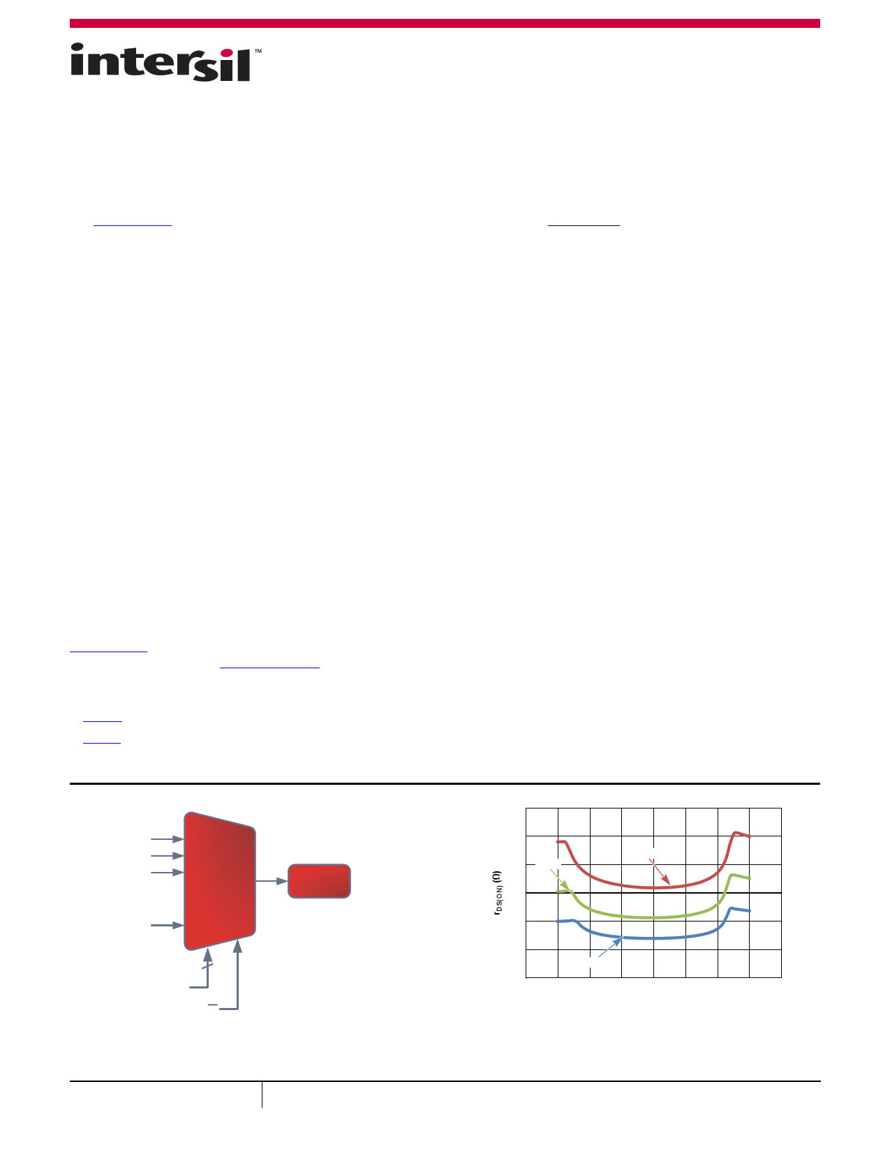
FIGURE 1. TYPICAL APPLICATION
June 15, 2015
FN8734.0
1
600
500
400 +25°C
+125°C
300
200
100
-55°C
0
-20 -15 -10 -5.0 0 5.0 10 15 20
SWITCH INPUT VOLTAGE (V)
FIGURE 2. rDS(ON) Vs POWER SUPPLY ACROSS SWITCH INPUT
COMMON MODE VOLTAGE AT +25°C
CAUTION: These devices are sensitive to electrostatic discharge; follow proper IC Handling Procedures.
1-888-INTERSIL or 1-888-468-3774 | Copyright Intersil Americas LLC 2015. All Rights Reserved
Intersil (and design) is a trademark owned by Intersil Corporation or one of its subsidiaries.
All other trademarks mentioned are the property of their respective owners.
1 page 
ISL71840SEH
Absolute Maximum Ratings
Positive Supply Voltage above GND (V+) (Note 5). . . . . . . . . . . . . . . . . +20V
Negative Supply Voltage below GND (V-) (Note 5 . . . . . . . . . . . . . . . . . .-20V
Maximum Supply Voltage Differential (V+ to V-) (Note 5) . . . . . . . . . . . 40V
Maximum Current Through Selected Switch. . . . . . . . . . . . . . . . . . . . 10mA
Analog Input Voltage (INx)
From GND (Note 5) . . . . . . . . . . . . . . . . . . . . . . . . . . . . . . . . . . . . . . . . ±35V
Digital Input Voltage Range (EN, Ax) . . . . . . . . . . . . . . . . . . . . . . . . GND to V+
VREF to GND (Note 5) . . . . . . . . . . . . . . . . . . . . . . . . . . . . . . . . . . . . . . . . .16.5V
ESD Tolerance
Human Body Model (Tested per MIL-PRF-883 3015.7). . . . . . . . . . . 8kV
Charged Device Model (Tested per MIL-PRF-883 3015.7) . . . . . . . 250V
Machine Model (Tested per MIL-PRF-883 3015.7) . . . . . . . . . . . . . 250V
Thermal Information
Thermal Resistance (Typical)
JA (°C/W) JC (°C/W)
28 Ld CDFP (Notes 3, 4) . . . . . . . . . . . . . . .
48
4
Storage Temperature Range. . . . . . . . . . . . . . . . . . . . . . . .-65°C to +150°C
Recommended Operating Conditions
Ambient Operating Temperature Range . . . . . . . . . . . . . .-55°C to +125°C
Maximum Operating Junction Temperature . . . . . . . . . . . . . . . . . .+150°C
Positive Supply Voltage Above GND (V+) . . . . . . . . . . . . . +10.8V to +16.5V
Negative Supply Voltage Below GND (V-) . . . . . . . . . . . . . . .-10.8V to -16.5V
Supply Voltage Differential (V+ to V-) . . . . . . . . . . . . . . . . . . . . 21.6V to 33V
VREF to GND . . . . . . . . . . . . . . . . . . . . . . . . . . . . . . . . . . . . . . . . . 4.5V to 5.5V
CAUTION: Do not operate at or near the maximum ratings listed for extended periods of time. Exposure to such conditions may adversely impact product
reliability and result in failures not covered by warranty.
NOTES:
3. JA is measured with the component mounted on a high effective thermal conductivity test board in free air. See Tech Brief TB379 for details.
4. For JC, the “case temp” location is the center of the package underside.
5. Tested in a heavy ion environment at LET = 86.3 MeV•cm2/mg at +125°C.
Electrical Specifications (15V) V+ = 15V, V- = -15V, VAH = 4V, VAL = 0.8V, VREF = VEN = 5V, TA= +25°C, unless otherwise noted.
Boldface limits apply across the operating temperature range, -55°C to +125°C or across a total ionizing dose of 300krad(Si) with exposure of a high
dose rate of 50 to 300krad(Si)/s or a total ionizing dose of 50krad(Si) with exposure at a low dose rate of <10mrad(Si)/s.
PARAMETER
VS
rON
DESCRIPTION
Analog Input Signal Range
Channel ON-resistance
ΔrON
RFLAT(ON)
IS(OFF)
rON Match Between Channels
ON-resistance Flatness
Switch Off Leakage
TEST CONDITIONS
V± = ±15.0V, ±16.5V
IOUT = -1mA, VIN = +5V, -5V
V± = ±15.0V, ±16.5V
IOUT = -1mA, VIN = V+, V-
VIN = +5V, -5V; IOUT = -1mA
VIN = +5V, -5V
VIN = V+ - 5V, V± = ±16.5V,
All unused inputs are tied to V- + 5V
MIN
(Note 6)
V-
-
MAX
TYP (Note 6)
- V+
- 500
UNIT
V
Ω
- - 700 Ω
- 10 20
- - 25
-10 - 10
Ω
Ω
nA
Post radiation
-100 - 100 nA
VIN = V- + 5V, V± = ±16.5V
All other inputs = V+ - 5V
TA = +25°C
TA = +125°C
Post radiation
-10 - 10 nA
-20 - 20 nA
-100 - 100 nA
IS(OFF) POWER OFF Switch Off Leakage with Device
Powered Off
VIN = +25V, V± = VEN = VA = VREF = 0V
TA = +25°C, V± = 0V
TA = -55°C, +125°C
Post radiation
-10 - 10 nA
-10 - 80 nA
-100 - 100 nA
VIN = -25V, V± = VEN = VA = VREF = 0V
TA = +25°C, V± = 0V
TA = -55°C, +125°C
Post radiation
-10 - 10 nA
-80 - 10 nA
-100 - 100 nA
Submit Document Feedback
5
FN8734.0
June 15, 2015
5 Page 
Timing Diagrams
ISL71840SEH
+4.0V
+0.8V
ISL71840SEH
50Ω
A3 IN01
A2
A1
IN02-IN15
A0 IN16
+0.8V EN
OUT
+15V, 0V
0V, +15V
10kΩ
VOUT
50pF
FIGURE 4. ADDRESS TIME TO OUTPUT TEST CIRCUIT
ISL71840SEH
A3 IN01
A2
A1
IN02-IN16
A0
+10V
+4.0V
+0.8V
EN
50Ω
OUT
VOUT
1kΩ 50pF
FIGURE 6. TIME TO ENABLE/DISABLE OUTPUT TEST CIRCUIT
+4.0V
+0.8V
ISL71840SEH
A3 IN01
A2
A1
IN02-IN15
50Ω A0
IN16
+5V
+0.8V EN
OUT
VOUT
1kΩ 50pF
FIGURE 8. BREAK-BEFORE-MAKE TEST CIRCUIT
+4.0V
+0.8V
ISL71840SEH
A3 IN01
A2
A1
IN02-IN15
50Ω A0 IN16
0V
+0.8V EN
OUT
VOUT
100pF
FIGURE 10. CHARGE INJECTION TEST CIRCUIT
4V
“11111”
ADDRESS
50%
50%
0.8V
15V
OUTPUT
“00000”
tAHL
50%
tALH
50%
0V
FIGURE 5. ADDRESS TIME TO OUTPUT DIAGRAM
4V
ENABLE
50%
50%
0.8V
10V
OUTPUT
tENABLE
50%
tDISABLE
50%
0V
FIGURE 7. TIME TO ENABLE/DISABLE OUTPUT DIAGRAM
4V
ADDRESS
0.8V
5V
OUT
50%
0V tBBM
FIGURE 9. BREAK-BEFORE-MAKE DIAGRAM
4V
ADDRESS
0.8V
15V
OUT
0V
Q = 100pF * ΔVOUT
ΔVOUT
FIGURE 11. CHARGE INJECTION DIAGRAM
Submit Document Feedback 11
FN8734.0
June 15, 2015
11 Page | ||
| Páginas | Total 27 Páginas | |
| PDF Descargar | [ Datasheet ISL71840SEH.PDF ] | |
Hoja de datos destacado
| Número de pieza | Descripción | Fabricantes |
| ISL71840SEH | Radiation Hardened 30V 16-Channel Analog Multiplexer | Intersil |
| Número de pieza | Descripción | Fabricantes |
| SLA6805M | High Voltage 3 phase Motor Driver IC. |
Sanken |
| SDC1742 | 12- and 14-Bit Hybrid Synchro / Resolver-to-Digital Converters. |
Analog Devices |
|
DataSheet.es es una pagina web que funciona como un repositorio de manuales o hoja de datos de muchos de los productos más populares, |
| DataSheet.es | 2020 | Privacy Policy | Contacto | Buscar |