|
|
|
PDF DS1086 Data sheet ( Hoja de datos )
| Número de pieza | DS1086 | |
| Descripción | Spread-Spectrum EconOscillator | |
| Fabricantes | Maxim Integrated | |
| Logotipo | ||
Hay una vista previa y un enlace de descarga de DS1086 (archivo pdf) en la parte inferior de esta página. Total 15 Páginas | ||
|
No Preview Available !
19-6224; Rev 2; 3/12
Spread-Spectrum EconOscillator
General Description
The DS1086 EconOscillator™ is a programmable clock
generator that produces a spread-spectrum (dithered)
square-wave output of frequencies from 260kHz to
133MHz. The selectable dithered output reduces radi-
ated-emission peaks by dithering the frequency 2% or
4% below the programmed frequency. The DS1086 has
a power-down mode and an output-enable control for
power-sensitive applications. All the device settings are
stored in nonvolatile (NV) EEPROM memory allowing it
to operate in stand-alone applications.
Applications
Printers
Copiers
PCs
Computer Peripherals
Cell Phones
Cable Modems
Features
o User-Programmable Square-Wave Generator
o Frequencies Programmable from 260kHz to
133MHz
o 2% or 4% Selectable Dithered Output
o Glitchless Output-Enable Control
o 2-Wire Serial Interface
o Nonvolatile Settings
o 5V Supply
o No External Timing Components Required
o Power-Down Mode
o 10kHz Master Frequency Step Size
o EMI Reduction
Ordering Information
PART
TEMP RANGE
PIN-PACKAGE
DS1086U
0°C to +70°C
8 µSOP
DS1086U+
0°C to +70°C
8 µSOP
DS1086Z
0°C to +70°C
8 SO
DS1086Z+
0°C to +70°C
8 SO
Note: Contact the factory for custom settings.
+Denotes a lead(Pb)-free/RoHS-compliant package.
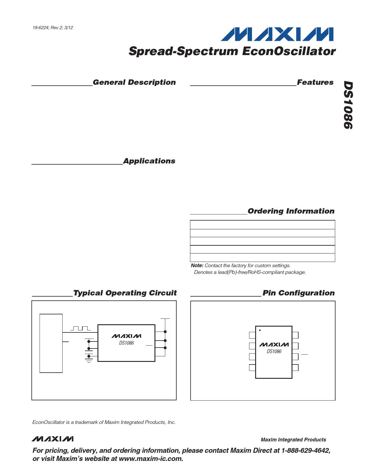
Typical Operating Circuit
Pin Configuration
MICRO-
PROCESSOR
DITHERED 260kHz TO
133MHz OUTPUT
XTL1/OSC1
VCC OUT
XTL2/OSC2 N.C.
SPRD
VCC
GND
DS1086
VCC
SCL*
SDA*
PDN
OE
DECOUPLING CAPACITORS
(0.1µF and 0.01µF)
*SDA AND SCL CAN BE CONNECTED DIRECTLY HIGH IF THE DS1086 NEVER NEEDS
TO BE PROGRAMMED IN-CIRCUIT, INCLUDING DURING PRODUCTION TESTING.
TOP VIEW
OUT 1
SPRD 2
VCC 3
GND 4
DS1086
8 SCL
7 SDA
6 PDN
5 OE
µSOP/SO
EconOscillator is a trademark of Maxim Integrated Products, Inc.
________________________________________________________________ Maxim Integrated Products 1
For pricing, delivery, and ordering information, please contact Maxim Direct at 1-888-629-4642,
or visit Maxim’s website at www.maxim-ic.com.
1 page 
Spread-Spectrum EconOscillator
AC ELECTRICAL CHARACTERISTICS: 2-WIRE INTERFACE (continued)
(VCC = 5V ±5%, TA = 0°C to +70°C.)
PARAMETER
Setup Time for STOP
Capacitive Load for Each Bus
Line
NV Write-Cycle Time
Input Capacitance
SYMBOL
tSU:STO
CONDITION
Fast mode
Standard mode
CB (Note 16)
tWR
CI
MIN TYP
0.6
4.0
5
MAX
400
10
UNITS
µs
pF
ms
pF
Note 1:
Note 2:
Note 3:
Note 4:
Note 5:
Note 6:
Note 7:
Note 8:
Note 9:
Note 10:
Note 11:
Note 12:
Note 13:
Note 14:
Note 15:
Note 16:
Note 17:
All voltages are referenced to ground.
DAC and OFFSET register settings must be configured to maintain the master oscillator frequency within this range.
Correct operation of the device is not guaranteed if these limits are exceeded.
This is the absolute accuracy of the master oscillator frequency at the default settings.
This is the change that is observed in master oscillator frequency with changes in voltage from nominal voltage at
TA = +25°C.
This is the percentage frequency change from the +25°C frequency due to temperature at VCC = 5V. The maximum tem-
perature change varies with the master oscillator frequency setting. The minimum occurs at the default master oscillator
frequency (fdefault). The maximum occurs at the extremes of the master oscillator frequency range (66MHz or 133MHz)
(see Figure 2).
The dither deviation of the master oscillator frequency is unidirectional and lower than the undithered frequency.
The integral nonlinearity of the frequency adjust DAC is a measure of the deviation from a straight line drawn between the
two endpoints of a range. The error is in percentage of the span.
This is true when the prescaler = 1.
Frequency settles faster for small changes in value. During a change, the frequency transitions smoothly from the original
value to the new value.
This indicates the time elapsed between power-up and the output becoming active. An on-chip delay is intentionally
introduced to allow the oscillator to stabilize. tstab is equivalent to approximately 512 master clock cycles and therefore
depends on the programmed clock frequency.
Output voltage swings can be impaired at high frequencies combined with high output loading.
A fast-mode device can be used in a standard-mode system, but the requirement tSU:DAT > 250ns must then be met.
This is automatically the case if the device does not stretch the LOW period of the SCL signal. If such a device does
stretch the LOW period of the SCL signal, it must output the next data bit to the SDA line at least tR MAX + tSU:DAT =
1000ns + 250ns = 1250ns before the SCL line is released.
After this period, the first clock pulse is generated.
A device must internally provide a hold time of at least 300ns for the SDA signal (referred to as the VIH MIN of the SCL sig-
nal) in order to bridge the undefined region of the falling edge of SCL.
The maximum tHD:DAT need only be met if the device does not stretch the LOW period (tLOW) of the SCL signal.
CB—total capacitance of one bus line, timing referenced to 0.9 x VCC and 0.1 x VCC.
Typical frequency shift due to aging is ±0.5%. Aging stressing includes Level 1 moisture reflow preconditioning (24hr
+125°C bake, 168hr 85°C/85%RH moisture soak, and 3 solder reflow passes +240 +0/-5°C peak) followed by 1000hr
max VCC biased 125°C HTOL, 1000 temperature cycles at -55°C to +125°C, 96hr 130°C/85%RH/5.5V HAST and 168hr
121°C/2 ATM Steam/Unbiased Autoclave.
_______________________________________________________________________________________ 5
5 Page 
Spread-Spectrum EconOscillator
must be read from the RANGE register (last five bits). In
this example, 12h (18 decimal) was read from the
RANGE register. OS - 2 for this case is 10h (16 deci-
mal). This is the value that is written to the OFFSET reg-
ister.
Finally, the two-byte DAC value needs to be deter-
mined. Since OS - 2 only sets the range of frequencies,
the DAC selects one frequency within that range as
shown in Equation 3.
fMASTER OSCILLATOR = (MIN FREQUENCY OF SELECTED OFFSET
RANGE) + (DAC value x 10kHz)
Valid values of DAC are 0 to 1023 (decimal) and 10kHz
is the step size. Equation 4 is derived from rearranging
Equation 3 and solving for DAC.
(fMASTER OSCILLATOR −
MIN FREQUENCY OF SELECTED
DAC VALUE =
OFFSET RANGE)
10kHz STEP SIZE
DAC VALUE = (88.4736MHz − 81.92MHz)
10kHz STEP SIZE
= 655.36 ≈ 655 (decimal)
(4)
Since the two-byte DAC register is left justified, 655 is
converted to hex (028Fh) and bit-wise shifted left six
places. The value to be programmed into the DAC reg-
ister is A3C0h.
In summary, the DS1086 is programmed as follows:
PRESCALER = 03h (4% peak dither) or 13h (2% peak
dither)
OFFSET = OS - 2 or 10h (if range was read as 12h)
DAC = A3C0h
Notice that the DAC value was rounded. Unfortunately,
this means that some error is introduced. In order to
calculate how much error, a combination of Equation 1
and Equation 3 is used to calculate the expected out-
put frequency. See Equation 5.
(MIN FREQUENCY OF SELECTED OFFSET
fOUTPUT
=
RANGE) + (DAC
VALUE x 10kHz STEP SIZE)
prescaler
fOUTPUT
= (81.92MHz) + (655 x 10kHz) =
8
88.47MHz = 11.05875MHz
8
(5)
The expected output frequency is not exactly equal to the
desired frequency of 11.0592MHz. The difference is
450Hz. In terms of percentage, Equation 6 shows that the
expected error is 0.004%. The expected error assumes
typical values and does not include deviations from the
typical as specified in the electrical tables.
%ERROREXPECTED
=
fDESIRED − fEXPECTED
fDESIRED
×
100
%ERROREXPECTED
=
11.0592MHz − 11.05875MHz
11.0592MHz
× 100 = 450Hz × 100 = 0.004%
11.0592MHz
(6)
Example #2: Calculate the register values needed to
generate a desired output frequency of 100MHz.
Since the desired frequency is already within the valid
master oscillator frequency range, the prescaler is set
to divide by 1, and hence, PRESCALER = 00h (for 4%
peak dither) or 10h (for 2% peak dither).
(7)
fMASTER OSCILLATOR = 100.0MHz x 20 = 100.0MHz
Next, looking at Table 2, OS + 1 provides a range of
frequencies centered around the desired frequency. In
order to determine what value to write to the OFFSET
register, the RANGE register must first be read.
Assuming 12h was read in this example, 13h (OS + 1)
is written to the OFFSET register.
Finally, the DAC value is calculated as shown in
Equation 8.
(8)
DAC VALUE = (100.0MHz − 97.28MHz) = 272.00 (decimal)
10kHz STEP SIZE
The result is then converted to hex (0110h) and then
left-shifted, resulting in 4400h to be programmed into
the DAC register.
In summary, the DS1086 is programmed as follows:
PRESCALER = 00h (4% peak dither) or 10h (2% peak
dither)
OFFSET = OS + 1 or 13h (if RANGE was read as 12h)
DAC = 4400h
fOUTPUT
=
(97.28MHz) + (272 × 10kHz)
20
=
100.0MHz = 100.0MHz
1
(9)
______________________________________________________________________________________ 11
11 Page | ||
| Páginas | Total 15 Páginas | |
| PDF Descargar | [ Datasheet DS1086.PDF ] | |
Hoja de datos destacado
| Número de pieza | Descripción | Fabricantes |
| DS1080CL | Spread-Spectrum Crystal Multiplier | Maxim Integrated Products |
| DS1080L | Spread-Spectrum Crystal Multiplier | Dallas Semiconductor |
| DS1081L | Spread-Spectrum Clock Modulator | Maxim Integrated Products |
| DS1085 | EconOscillator Frequency Synthesizer | Dallas Semiconductor |
| Número de pieza | Descripción | Fabricantes |
| SLA6805M | High Voltage 3 phase Motor Driver IC. |
Sanken |
| SDC1742 | 12- and 14-Bit Hybrid Synchro / Resolver-to-Digital Converters. |
Analog Devices |
|
DataSheet.es es una pagina web que funciona como un repositorio de manuales o hoja de datos de muchos de los productos más populares, |
| DataSheet.es | 2020 | Privacy Policy | Contacto | Buscar |