|
|
|
PDF IRFB7430PBF Data sheet ( Hoja de datos )
| Número de pieza | IRFB7430PBF | |
| Descripción | Power MOSFET ( Transistor ) | |
| Fabricantes | International Rectifier | |
| Logotipo | ||
Hay una vista previa y un enlace de descarga de IRFB7430PBF (archivo pdf) en la parte inferior de esta página. Total 9 Páginas | ||
|
No Preview Available !
Applications
l Brushed Motor drive applications
l BLDC Motor drive applications
l Battery powered circuits
l Half-bridge and full-bridge topologies
l Synchronous rectifier applications
l Resonant mode power supplies
l OR-ing and redundant power switches
l DC/DC and AC/DC converters
l DC/AC Inverters
Benefits
l Improved Gate, Avalanche and Dynamic dV/dt
Ruggedness
l Fully Characterized Capacitance and Avalanche
SOA
l Enhanced body diode dV/dt and dI/dt Capability
l Lead-Free
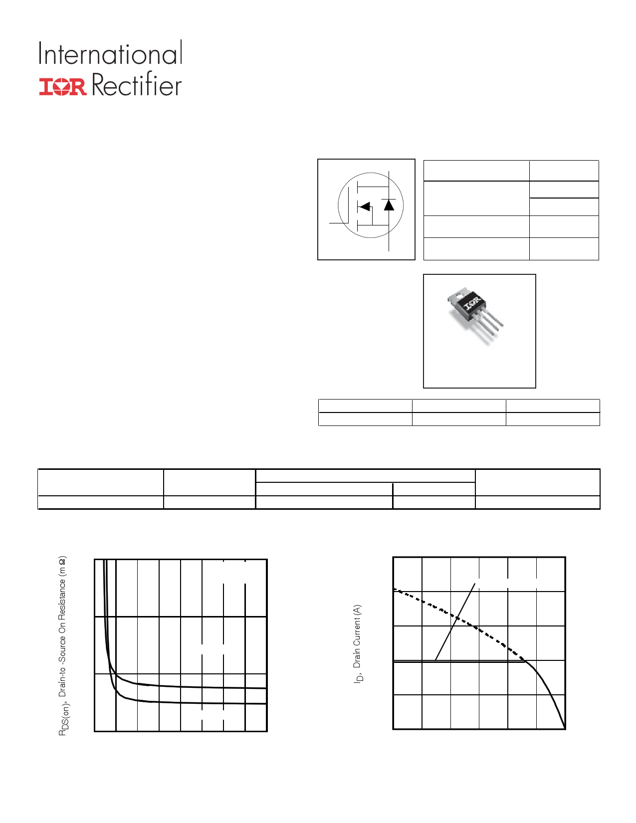
PD - 97782A
StrongIRFET
IRFB7430PbF
HEXFET® Power MOSFET
D VDSS
40V
RDS(on) typ.
1.0m
cG max. 1.3m
ID (Silicon Limited)
409A
S
ID (Package Limited)
195A
D
G
Gate
DS
G
TO-220AB
IRFB7430PbF
D
Drain
S
Source
Ordering Information
Base Part Number
IRFB7430PbF
Package Type
TO-220
Standard Pack
Form
Tube
Qua nti ty
50
Complete Part Number
IRFB7430PbF
6.0
ID = 100A
4.0
TJ = 125°C
2.0
TJ = 25°C
0.0
4 6 8 10 12 14 16 18 20
VGS, Gate -to -Source Voltage (V)
Fig 1. Typical On-Resistance vs. Gate Voltage
www.irf.com
500
Limited By Package
400
300
200
100
0
25 50 75 100 125 150 175
TC , Case Temperature (°C)
Fig 2. Maximum Drain Current vs. Case Temperature
1
05/22/12
1 page 
1000
100 TJ = 175°C
10
TJ = 25°C
1
VGS = 0V
0.1
0.0 0.5 1.0 1.5 2.0
VSD, Source-to-Drain Voltage (V)
Fig 9. Typical Source-Drain Diode
Forward Voltage
47
Id = 1.0mA
46
2.5
45
44
43
42
41
40
-60 -40 -20 0 20 40 60 80 100120140160180
TJ , Temperature ( °C )
Fig 11. Drain-to-Source Breakdown Voltage
6.0
4.0
IRFB7430PbF
10000
1000
OPERATION IN THIS AREA
LIMITED BY R DS(on)
100μsec
1msec
100
Limited by package
10
10msec
1 Tc = 25°C
Tj = 175°C
Single Pulse
0.1
0.1 1
DC
10 100
VDS, Drain-toSource Voltage (V)
Fig 10. Maximum Safe Operating Area
2.5
VDS= 0V to 32V
2.0
1.5
1.0
0.5
0.0
0 5 10 15 20 25 30 35 40 45
VDS, Drain-to-Source Voltage (V)
Fig 12. Typical COSS Stored Energy
VGS = 5.5V
VGS = 6.0V
VGS = 7.0V
VGS = 8.0V
VGS =10V
2.0
www.irf.com
0.0
0
200 400 600 800 1000 1200
ID, Drain Current (A)
Fig 13. Typical On-Resistance vs. Drain Current
5
5 Page | ||
| Páginas | Total 9 Páginas | |
| PDF Descargar | [ Datasheet IRFB7430PBF.PDF ] | |
Hoja de datos destacado
| Número de pieza | Descripción | Fabricantes |
| IRFB7430PBF | Power MOSFET ( Transistor ) | International Rectifier |
| Número de pieza | Descripción | Fabricantes |
| SLA6805M | High Voltage 3 phase Motor Driver IC. |
Sanken |
| SDC1742 | 12- and 14-Bit Hybrid Synchro / Resolver-to-Digital Converters. |
Analog Devices |
|
DataSheet.es es una pagina web que funciona como un repositorio de manuales o hoja de datos de muchos de los productos más populares, |
| DataSheet.es | 2020 | Privacy Policy | Contacto | Buscar |