|
|
|
PDF RT8475 Data sheet ( Hoja de datos )
| Número de pieza | RT8475 | |
| Descripción | High Voltage High Current LED Driver Controller | |
| Fabricantes | Richtek | |
| Logotipo | ||
Hay una vista previa y un enlace de descarga de RT8475 (archivo pdf) en la parte inferior de esta página. Total 16 Páginas | ||
|
No Preview Available !
®
RT8475
High Voltage High Current LED Driver Controller for
Buck, Boost or Buck-Boost Topology
General Description
The RT8475 is a current mode PWM controller designed
to drive an external MOSFET for high current LED
applications. With a current sense amplifier threshold of
190mV, the LED current is programmable with one
external current sense resistor. With the maximum
operating input voltage of 36V and output voltage up to
90V, the RT8475 is ideal for buck, boost or buck-boost
operation.
With the switching frequency programmable over 100kHz
to 1MHz, the external inductor and capacitors can be small
while maintaining high efficiency.
Dimming can be done by either analog or digital. The built-
in clamping comparator and filter allow easy low noise
analog dimming conversion from digital signal with only
one external capacitor.
The RT8475 is available in SOP-14 and WQFN-16L 3x3
packages.
Ordering Information
RT8475
Package Type
S : SOP-14
QW : WQFN-16L 3x3 (W-Type)
Lead Plating System
G : Green (Halogen Free and Pb Free)
Z : ECO (Ecological Element with
Halogen Free and Pb free)
Note :
Richtek products are :
` RoHS compliant and compatible with the current require-
ments of IPC/JEDEC J-STD-020.
` Suitable for use in SnPb or Pb-free soldering processes.
Features
z High Voltage Capability : VIN Up to 36V, LED Sensing
Threshold Common Mode Voltage Up to 90V
z Buck, Boost or Buck-Boost Operation
z Programmable Switching Frequency
z Easy Dimming Control : Analog or Digital
Converting to Analog with One External Capacitor
z Programmable Soft-Start to Avoid Inrush Current
z Programmable Over Voltage Protection
z VIN Under Voltage Lockout and Thermal Shutdown
z RoHS Compliant and Halogen Free
Applications
z General Industrial High Power LED Lighting
z Desk Lights and Room Lighting
z Building and Street Lighting
z Industrial Display Backlight
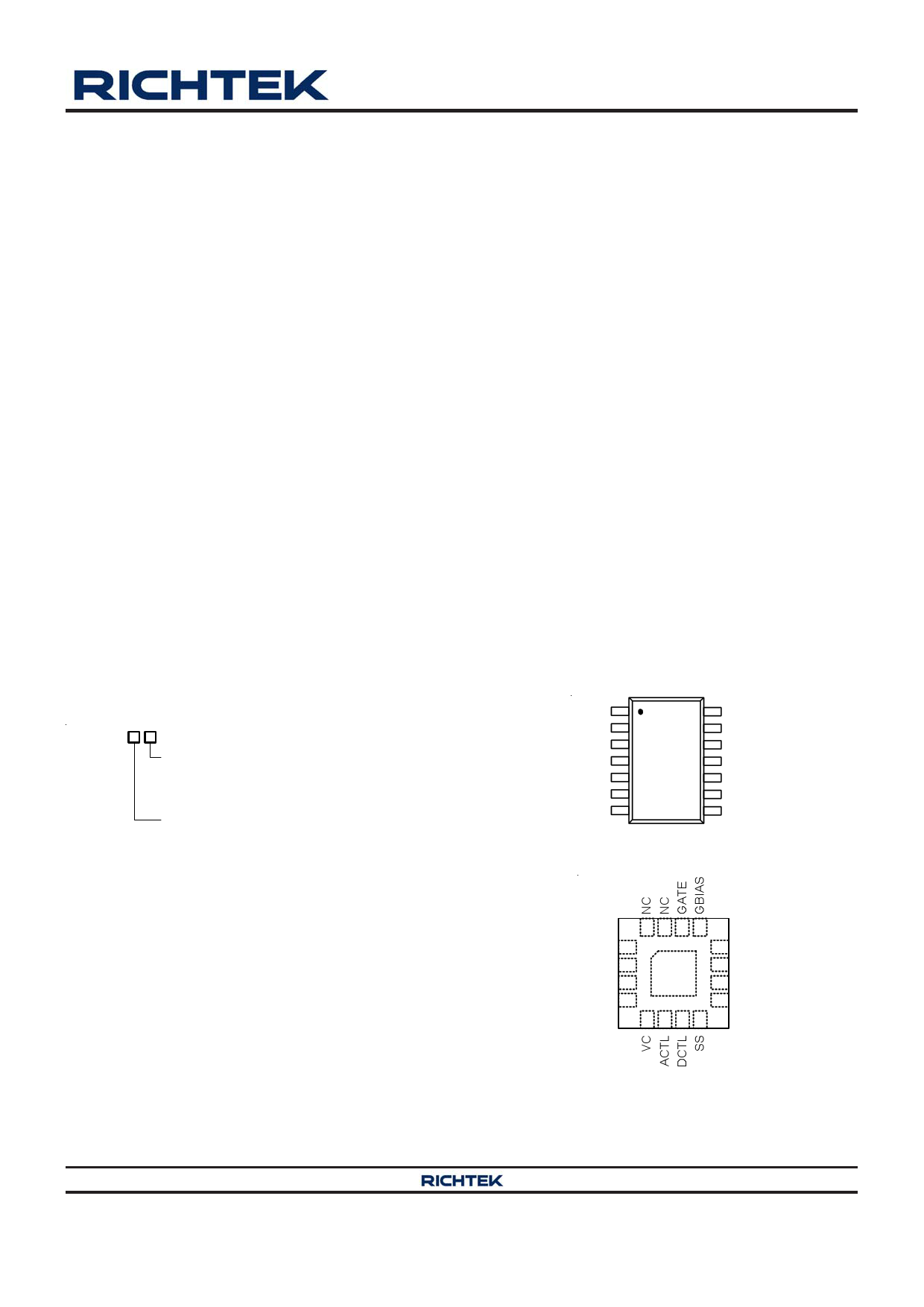
Pin Configurations
(TOP VIEW)
RSET
ISW
ISP
ISN
VC
ACTL
DCTL
2
3
4
5
6
7
14 GATE
13 GBIAS
12 GND
11 VCC
10 OVP
9 EN
8 SS
SOP-14
16 15 14 13
RSET
ISW
ISP
ISN
1
2
3
4
GND
17
12 GND
11 VCC
10 OVP
9 EN
5 678
WQFN-16L 3x3
Copyright ©2012 Richtek Technology Corporation. All rights reserved.
DS8475-03 October 2012
is a registered trademark of Richtek Technology Corporation.
www.richtek.com
1
1 page 
RT8475
Absolute Maximum Ratings (Note 1)
z Supply Input Voltage, VCC ---------------------------------------------------------------------------------------------- −0.3 to 38V
z GBIAS, GATE -------------------------------------------------------------------------------------------------------------- −0.3 to 10V
z ISW --------------------------------------------------------------------------------------------------------------------------- −0.3 to 1V
z ISP, ISN ---------------------------------------------------------------------------------------------------------------------- −0.3 to 100V
z DCTL, ACTL, OVP (Note 2) ------------------------------------------------------------------------------------------- −0.3 to 8V
z EN ----------------------------------------------------------------------------------------------------------------------------- −0.3 to 20V
z SS, RSET, VC -------------------------------------------------------------------------------------------------------------- −0.3 to 5V
z Power Dissipation, PD @ TA = 25°C
SOP-14 ---------------------------------------------------------------------------------------------------------------------- 1.0W
WQFN-16L 3x3 ------------------------------------------------------------------------------------------------------------ 1.471W
z Package Thermal Resistance (Note 3)
SOP-14, θJA ----------------------------------------------------------------------------------------------------------------- 100°C/W
WQFN-16L 3x3, θJA ------------------------------------------------------------------------------------------------------- 68°C/W
WQFN-16L 3x3, θJC ------------------------------------------------------------------------------------------------------ 7.5°C/W
z Junction Temperature ----------------------------------------------------------------------------------------------------- 150°C
z Lead Temperature (Soldering, 10 sec.) ------------------------------------------------------------------------------- 260°C
z Storage Temperature Range -------------------------------------------------------------------------------------------- −65°C to 150°C
z ESD Susceptibility (Note 4)
HBM (Human Body Model) ---------------------------------------------------------------------------------------------- 2kV
MM (Machine Model) ----------------------------------------------------------------------------------------------------- 200V
Recommended Operating Conditions (Note 5)
z Supply Input Voltage Range, VCC ------------------------------------------------------------------------------------- 4.5V to 36V
z Junction Temperature Range -------------------------------------------------------------------------------------------- −40°C to 125°C
Electrical Characteristics
(VCC = 24V, No Load on any Output, TA = 25°C, unless otherwise specified)
Parameter
Symbol
Test Conditions
Overall
Supply Current
Shutdown Current
EN Threshold
Voltage
Logic-High
Logic-Low
EN Input Current
IVCC
ISHDN
VIH
VIL
VVC ≤ 0.4V (Switching off)
VEN ≤ 0.7V
VEN ≤ 3V
Current Sense Amplifier
Input Threshold (VISP − VISN)
ISP Input Current
IISP
ISN Input Current
IISN
VC Output Current
IVC
VC Threshold for PWM Switch Off
VACTL ≥ 1.25V,
12V ≤ common mode ≤ 90V
VACTL ≥ 1.2V,
12V ≤ common mode ≤ 90V
4.5V ≤ VISP ≤ 90V
4.5V ≤ VISN ≤ 90V
0.5V ≤ VC ≤ 2.4V
Min Typ Max Unit
-- 6 7.2 mA
-- 12 -- μA
2 -- --
V
-- -- 0.5
-- -- 1.2 μA
182 190 198
mV
-- 188 --
-- 140 --
-- 60 --
-- ±20 --
-- 0.7 --
μA
μA
μA
V
Copyright ©2012 Richtek Technology Corporation. All rights reserved.
DS8475-03 October 2012
is a registered trademark of Richtek Technology Corporation.
www.richtek.com
5
5 Page 
The ACTL pin can also be used in conjunction with a
thermistor to provide over temperature protection for the
LED load, or with a voltage divider to VIN to reduce output
power and switching current when VIN is low. The presence
of a time varying differential voltage signal (ripple) across
ISP and ISN at the switching frequency is expected.
The amplitude of this signal is increased by high LED load
current, low switching frequency and/or a smaller value
output filter capacitor. The compensation capacitor on the
VC pin filters the signal so the average difference between
ISP and ISN is regulated on the user-programmed value.
Programmable Switching Frequency
The RSET frequency adjust pin allows the user to program
the switching frequency from 100kHz to 1MHz for optimized
efficiency and performance or external component size.
Higher frequency operation allows for smaller component
size but increases switching losses and gate driving
current, and may not allow sufficiently high or low duty
cycle operation. Lower frequency operation gives better
performance but with larger external component size. For
an appropriate RRSET resistor value see Table 1 or Figure
5. An external resistor from the RSET pin to GND is
required-do not leave this pin open.
Table 1. Switching Frequency vs. RREST Value (1%
Resistor)
fOSC (kHZ)
1000
800
600
500
300
200
100
RRSET (kΩ)
8.34
11.41
16.68
20.9
38.04
60.35
130
RT8475
Frequency vs. RRSET
1000
900
800
700
600
500
400
300
200
100
0
0 15 30 45 60 75 90 105 120 135
RRRRSET (kΩΩ)
Figure 5. Switching Frequency vs. RRSET
Output Over Voltage Setting
The RT8475 is equipped with Over Voltage Protection
(OVP) function. When the voltage at OVP pin exceeds a
threshold of approximately1.2V, the power switch is turned
off. The power switch can be turned on again once the
voltage at OVP pin drops below 1.2V. For the Boost and
Buck-Boost application, the output voltage could be
clamped at a certain voltage level. The OVP voltage can
be set by the following equation :
VOUT,
OVP
=
1.2 × ⎛⎜⎝1+
R1 ⎞
R2 ⎟⎠
Where,
R1 and R2 are the voltage dividers from VOUT to GND with
the divider center node connected to OVP pin.
ISW Sense Resistor Selection
The resistor, RSW, between the source of the external
N-MOSFET and GND should be selected to provide
adequate switch current to drive the application without
exceeding the 110mV (typical) current limit threshold on
the ISW pin of RT8475. For real applications, select a
resistor that gives a switch current at least 30% greater
than the required LED current.
For Buck application, select a resistor according to :
RSW, Buck
=
⎛
⎜⎝
0.08V
IOUT
⎞
⎟⎠
Copyright ©2012 Richtek Technology Corporation. All rights reserved.
DS8475-03 October 2012
is a registered trademark of Richtek Technology Corporation.
www.richtek.com
11
11 Page | ||
| Páginas | Total 16 Páginas | |
| PDF Descargar | [ Datasheet RT8475.PDF ] | |
Hoja de datos destacado
| Número de pieza | Descripción | Fabricantes |
| RT8470 | High Brightness LED Driver | Richtek |
| RT8471 | High Brightness LED Driver | Richtek |
| RT8472 | High Brightness LED Driver | Richtek |
| RT8473 | High Brightness LED Driver | Richtek |
| Número de pieza | Descripción | Fabricantes |
| SLA6805M | High Voltage 3 phase Motor Driver IC. |
Sanken |
| SDC1742 | 12- and 14-Bit Hybrid Synchro / Resolver-to-Digital Converters. |
Analog Devices |
|
DataSheet.es es una pagina web que funciona como un repositorio de manuales o hoja de datos de muchos de los productos más populares, |
| DataSheet.es | 2020 | Privacy Policy | Contacto | Buscar |