|
|
|
PDF ISL6617 Data sheet ( Hoja de datos )
| Número de pieza | ISL6617 | |
| Descripción | PWM Doubler | |
| Fabricantes | Intersil Corporation | |
| Logotipo | ||
Hay una vista previa y un enlace de descarga de ISL6617 (archivo pdf) en la parte inferior de esta página. Total 15 Páginas | ||
|
No Preview Available !
PWM Doubler with Phase Shedding Function and
Output Monitoring Feature
ISL6617
The ISL6617 utilizes Intersil’s proprietary Phase Doubler
scheme to modulate two-phase power trains with single
PWM input. It doubles the number of phases that
Intersil’s multi-phase controllers ISL63xx can support.
When the enable pin (EN_PH_SYNC) is pulled low, the
PWM input is pulled high. This simplifies the phase
shedding implementation for some Intersil controllers
(VR10, VR11, VR11.1, and VR12 family) that can disable
the respective and higher phase(s) by pulling the
respective PWM line high.
The ISL6617 is designed to minimize the number of
analog signals that interface between the controller and
drivers in high phase count scalable applications. The
common COMP signal, which is usually seen in
conventional cascaded configuration, is not required; this
improves noise immunity and simplifies the layout.
Furthermore, the ISL6617 provides low part count and
low cost advantage over the conventional cascaded
technique.
By cascading the ISL6617 with another ISL6617 or
ISL6611A, it can quadruple the number of phases that
Intersil’s multi-phase controllers ISL63xx can support.
The ISL6617 also features Tri-State input and outputs
that recognize a high-impedance state, working together
with Intersil multiphase PWM controllers and driver
stages to prevent negative transients on the controlled
output voltage when operation is suspended. This feature
eliminates the need for the schottky diode that may be
utilized in a power system to protect the load from
excessive negative output voltage damage.
Features
• Proprietary Phase Doubler scheme with Phase
Shedding Function (Patent Pending)
• Enhanced Light to Full Load Efficiency
• Double or Quadruple Phase Count
• Patented Current Balancing with DCR Current
Sensing and Adjustable Gain
• Current Monitoring Output (IOUT) to Simplify
System Interface and Layout
• Triple-Level Enable Input for Mode Selection
• Dual PWM Output Drives for Two Synchronous
Rectified Bridges with Single PWM Input
• Channel Synchronization and Two Interleaving Options
• Tri-State PWM Input and Outputs for Output Stage
Shutdown
• Phase Enable Input and PWM Forced High Output to
Interface with Intersil’s Controller for Phase Shedding
• Overvoltage Protection
• Dual Flat No-Lead (DFN) Package
- Near Chip-Scale Package Footprint; Improves PCB
Utilization, Thinner Profile
- Pb-Free (RoHS Compliant)
Related Literature
• Technical Brief TB363 “Guidelines for Handling and
Processing Moisture Sensitive Surface Mount Devices
(SMDs)”
Applications
• High Current Low Voltage DC/DC Converters
• High Frequency and High Efficiency VRM and VRD
• High Phase Count and Phase Shedding Applications
• 5V PWM Input Integrated Power Stage or DrMOS
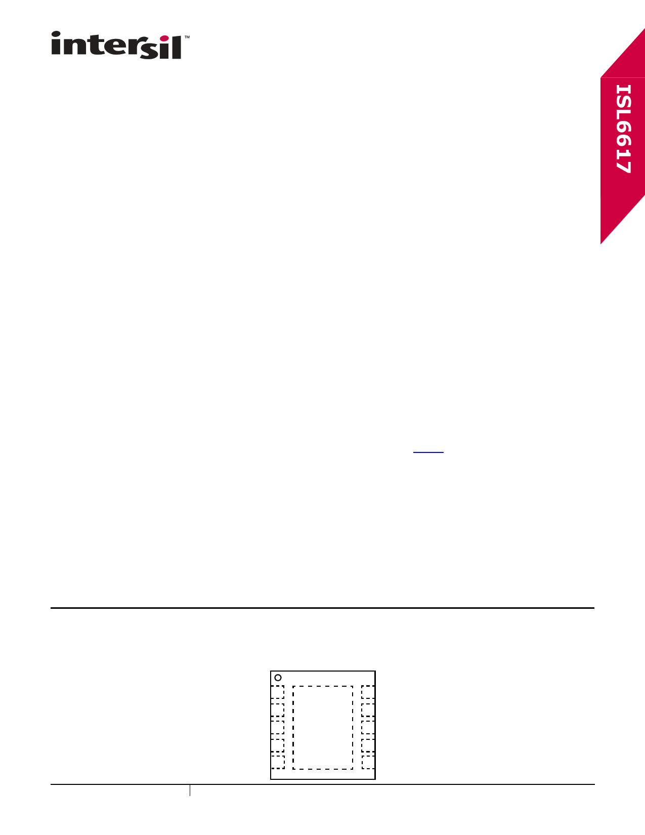
Pin Configuration
ISL6617
(10 LD DFN)
TOP VIEW
February 4, 2010
FN7564.0
ISENA+ 1
ISENA- 2
PWMIN 3
ISENB+ 4
ISENB- 5
11
GND
10 PWMA
9 VCC
8 IOUT
7 EN_PH_SYNC
6 PWMB
1 CAUTION: These devices are sensitive to electrostatic discharge; follow proper IC Handling Procedures.
1-888-INTERSIL or 1-888-468-3774 | Copyright Intersil Americas Inc. 2010. All Rights Reserved
Intersil (and design) is a trademark owned by Intersil Corporation or one of its subsidiaries.
All other trademarks mentioned are the property of their respective owners.
1 page 
ISL6617
Ordering Information
PART NUMBER
(Notes 1, 2, 3)
PART
MARKING
TEMP. RANGE
(°C)
PACKAGE
(Pb-Free)
PKG.
DWG. #
ISL6617CRZ
617C
0 to +70
10 Ld 3x3 DFN
L10.3x3
ISL6617IRZ
617I
-40 to +85
10 Ld 3x3 DFN
L10.3x3
NOTES:
1. Add “-T*” suffix for tape and reel. Please refer to TB347 for details on reel specifications.
2. These Intersil Pb-free plastic packaged products employ special Pb-free material sets, molding compounds/die attach
materials, and 100% matte tin plate plus anneal (e3 termination finish, which is RoHS compliant and compatible with both
SnPb and Pb-free soldering operations). Intersil Pb-free products are MSL classified at Pb-free peak reflow temperatures that
meet or exceed the Pb-free requirements of IPC/JEDEC J STD-020.
3. For Moisture Sensitivity Level (MSL), please see device information page for ISL6617. For more information on MSL, please
see Technical Brief TB363.
5 FN7564.0
February 4, 2010
5 Page 
ISL6617
When the doubler operates in interleaving mode, the
PWM controller frequency should be set at two times the
desired phase frequency (FSW). Since the input PWM
pulse is divided into half to feed into each phase of the
doubler, the operational duty cycle of each phase should
be less than 50%. In synchronous mode, the PWM
controller should be operated at the same frequency as
the desired phase frequency. In this mode, the allowable
duty cycle is up to 100%. For cascaded interleaving, the
controller switching frequency needs to be set at four
times the phase frequency. During cascaded operation,
the maximum allowable duty cycle will be less than 25%.
All of the maximum allowable duty cycle numbers
referenced assume that the PWM controller can send out
a 100% duty cycle pulse. In many cases, this is not
achievable because the controller needs time to reset it's
internal sawtooth ramp or internal max duty limit.
However, the fixed 120ns extension of interleaving mode
2 helps recover the typical 1% duty cycle loss associated
with the ramp reset time. In addition, Intersil has
developed a dedicated controller, the ISL6336G with
90% duty cycle, to work with the ISL6617 for high-phase
count and overclocking applications.
PWM1
PWMA
PWM1A
PWM1B
PWMB
PWM1C
PWM1D
FIGURE 9. CASCADED DOUBLER OPERATIONAL
WAVEFORMS
To properly compensate the system that uses phase
doublers, the effective system sawtooth to calculate the
modulator gain should factor in the duty cycle limitation
(DMAX) as Equation 1. For instance, when using
ISL6336G and ISL6617s in cascaded interleaving mode,
the effective sawtooth amplitude should be scaled as
3V/22.5% = 13.33V.
VRAMP_EFFECTIVE = V--D---R--M--A---A-M---X--P--
(EQ. 1)
Current Sensing
The ISL6617 senses current continuously for fast
response. The ISL6617 supports inductor DCR sensing,
or resistive sensing techniques. The associated channel
current sense amplifier uses the ISEN inputs to
reproduce a signal proportional to the inductor current,
IL. The sensed current, ISEN, is proportional to the
inductor current. The sensed current is used for current
balance and load-line regulation.
The internal circuitry, shown in Figures 10 and 11,
represents one channel. This circuitry is repeated for
each channel in the doubler. The input bias current of the
current sensing amplifier is typically 60nA; less than 5kΩ
input impedance is preferred to minimize the offset error.
In addition, the common mode input voltage to the
amplifier should be less than VCC-3V.
A. INDUCTOR DCR SENSING
An inductor’s winding is characteristic of a distributed
resistance, as measured by the DCR (Direct Current
Resistance) parameter. Consider the inductor DCR as a
separate lumped quantity, as shown in Figure 10.
VIN
IL(s)
POWER
STAGE
L DCR
INDUCTOR
VL
VOUT
COUT
VC(s)
PWMA/B
RC
ISL6617
IA/B
RISEN(A/B)
CURRENT
SENSE
+ ISEN-(A/B)
-
ISEN+(A/B)
CT
ISEN = IL -R--D--I--SC----E-R---N--
FIGURE 10. DCR SENSING CONFIGURATION
The channel current IL, flowing through the inductor, will
also pass through the DCR. Equation 2 shows the s-
domain equivalent voltage across the inductor VL.
VL(s) = IL ⋅ (s ⋅ L + DCR)
(EQ. 2)
A simple R-C network across the inductor extracts the
DCR voltage, as shown in Figure 10.
The voltage on the capacitor VC, can be shown to be
proportional to the channel current IL. See Equation 3.
VC(s)
=
⎝⎛s ⋅ D-----C-L----R--- + 1⎠⎞ ⋅ (DCR ⋅ IL)
--------------------(--s-----⋅---R----C------+-----1----)-------------------
(EQ. 3)
If the R-C network components are selected such that
the RC time constant matches the inductor time constant
(RC = L/DCR), the voltage across the capacitor VC is
equal to the voltage drop across the DCR, i.e.,
proportional to the channel current.
With the internal low-offset current amplifier, the
capacitor voltage VC is replicated across the sense
11 FN7564.0
February 4, 2010
11 Page | ||
| Páginas | Total 15 Páginas | |
| PDF Descargar | [ Datasheet ISL6617.PDF ] | |
Hoja de datos destacado
| Número de pieza | Descripción | Fabricantes |
| ISL6610 | Dual Synchronous Rectified MOSFET Drivers | Intersil Corporation |
| ISL6610A | Dual Synchronous Rectified MOSFET Drivers | Intersil Corporation |
| ISL6611A | Phase Doubler | Intersil Corporation |
| ISL6612 | (ISL6612 / ISL6613) Advanced Synchronous Rectified Buck MOSFET Drivers | Intersil Corporation |
| Número de pieza | Descripción | Fabricantes |
| SLA6805M | High Voltage 3 phase Motor Driver IC. |
Sanken |
| SDC1742 | 12- and 14-Bit Hybrid Synchro / Resolver-to-Digital Converters. |
Analog Devices |
|
DataSheet.es es una pagina web que funciona como un repositorio de manuales o hoja de datos de muchos de los productos más populares, |
| DataSheet.es | 2020 | Privacy Policy | Contacto | Buscar |