|
|
|
PDF T320XVN02.0-SKD Data sheet ( Hoja de datos )
| Número de pieza | T320XVN02.0-SKD | |
| Descripción | TFT LCD Module | |
| Fabricantes | AUO | |
| Logotipo | ||
Hay una vista previa y un enlace de descarga de T320XVN02.0-SKD (archivo pdf) en la parte inferior de esta página. Total 23 Páginas | ||
|
No Preview Available !
T320XVN02.0 SKD Product Spec.
Rev.1.0
Model Name: T320XVN02.0 (SKD)
Issue Date : 2012/01/16
( )Preliminary Specifications
(*)Final Specifications
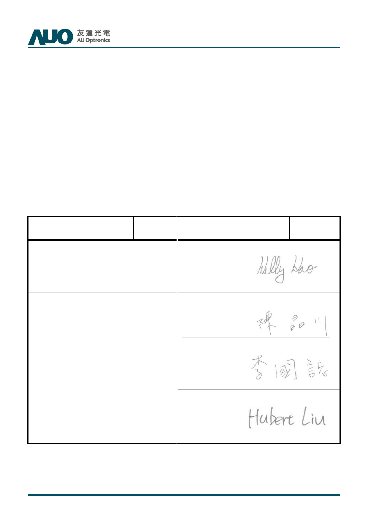
Customer Signature
Date AUO
Date
Approved By
_________________________________
Approval By PM Director
Kelly Kao
____________________________________
Note
Reviewed By RD Director
Eugene CC Chen
____________________________________
Reviewed By Project Leader
Kuo Chih Lee
____________________________________
Prepared By PM
Hubert Liu
____________________________________
© Copyright AUO Optronics Corp. 2009 All Rights Reserved.
Page 1 / 23
1 page 
2. Absolute Maximum Ratings
T320XVN02.0 SKD Product Spec.
Rev.1.0
The followings are maximum values which, if exceeded, may cause faulty operation or damage to the unit
Item
Logic/LCD Drive Voltage
Input Voltage of Signal
Operating Temperature
Operating Humidity
Storage Temperature
Storage Humidity
Panel Surface Temperature
Symbol
Vcc
Vin
TOP
HOP
TST
HST
PST
Min
-0.3
-0.3
0
10
-20
10
Max
14
4
+50
90
+60
90
65
Unit
[Volt]
[Volt]
[oC]
[%RH]
[oC]
[%RH]
[oC]
Conditions
Note 1
Note 1
Note 2
Note 2
Note 2
Note 2
Note 3
Note 1: Duration:50 msec.
℃Note 2 : Maximum Wet-Bulb should be 39 and No condensation.
℃The relative humidity must not exceed 90% non-condensing at temperatures of 40 or less. At temperatures
℃ ℃greater than 40 , the wet bulb temperature must not exceed 39 .
℃Note 3: Surface temperature is measured at 50 Dry condition
© Copyright AUO Optronics Corp. 2009 All Rights Reserved.
Page 5 / 23
5 Page 
3.2 Signal Timing Specification
T320XVN02.0 SKD Product Spec.
Rev.1.0
This is the signal timing required at the input of the user connector. All of the interface signal timing should be
satisfied with the following specifications for its proper operation.
Timing Table (DE only Mode)
Signal
Item
Vertical Section
Period
Active
Blanking
Period
Horizontal Section
Active
Blanking
Clock
Frequency
Vertical Frequency
Frequency
Horizontal Frequency Frequency
Symbol
Tv
Tdisp (v)
Tblk (v)
Th
Tdisp (h)
Tblk (h)
Fclk=1/Tclk
Fv
Fh
Min.
784
16
1460
94
50
47
43
Typ.
810
768
42
1648
1366
282
80
60
48
Max
1015
Unit
Th
247
2000
Th
Tclk
634 Tclk
86 MHz
63 Hz
53 KHz
Notes:
(1) Display position is specific by the rise of DE signal only.
Horizontal display position is specified by the rising edge of 1st DCLK after the rise of 1st DE, is displayed on the
left edge of the screen.
(2)Vertical display position is specified by the rise of DE after a “Low” level period equivalent to eight times of
horizontal period. The 1st data corresponding to one horizontal line after the rise of 1st DE is displayed at the top
line of screen.
(3)If a period of DE “High” is less than 1366 DCLK or less than 768 lines, the rest of the screen displays black.
(4)The display position does not fit to the screen if a period of DE “High” and the effective data period do not
synchronize with each other.
© Copyright AUO Optronics Corp. 2009 All Rights Reserved.
Page 11 / 23
11 Page | ||
| Páginas | Total 23 Páginas | |
| PDF Descargar | [ Datasheet T320XVN02.0-SKD.PDF ] | |
Hoja de datos destacado
| Número de pieza | Descripción | Fabricantes |
| T320XVN02.0-SKD | TFT LCD Module | AUO |
| Número de pieza | Descripción | Fabricantes |
| SLA6805M | High Voltage 3 phase Motor Driver IC. |
Sanken |
| SDC1742 | 12- and 14-Bit Hybrid Synchro / Resolver-to-Digital Converters. |
Analog Devices |
|
DataSheet.es es una pagina web que funciona como un repositorio de manuales o hoja de datos de muchos de los productos más populares, |
| DataSheet.es | 2020 | Privacy Policy | Contacto | Buscar |