|
|
|
PDF MB86605 Data sheet ( Hoja de datos )
| Número de pieza | MB86605 | |
| Descripción | Wide SCSI-II Protocol Controller | |
| Fabricantes | Fujitsu Media Devices | |
| Logotipo | ||
Hay una vista previa y un enlace de descarga de MB86605 (archivo pdf) en la parte inferior de esta página. Total 30 Páginas | ||
|
No Preview Available !
FUJITSU SEMICONDUCTOR
DATA SHEET
ASSP Communication Control
CMOS
Wide SCSI-II Protocol Controller
With PCI Interface
MB86605
DS04-22416-1E
s DESCRIPTION
The MB86605 is an intelligent SCSI Protocol Controller (SPC) which complies with ANSI (SCSI-2) standard and
integrates a PCI local bus interface function. The specification of SCSI controller block is based on the MB86603
which is a wide SCSI-2 protocol controller with addition of some enhancements such as integration of PCI
interface, enlarged “user program memory” (2 KBytes) and improvement of internal operation speed and
performance. The MB86605 is capable of transferring up to 20 Mbyte/sec at the wide high speed synchronous
mode. As for the SCSI bus pins, a totem pole type single-ended driver/receiver is incorporated in the device so
that it can drive the SCSI bus directly. Furthermore, the MB86605 is capable of connecting the external differential
type driver/receiver.
The SCSI bus sequence is controlled by commands issued from a host system. So, it supports sequential
commands that perform the phase-to-phase sequences to reduce the system overhead of sequence operations.
As another key feature to reduce the system overhead, the device has a 2 Kbytes user program memory to store
user program codes. Due to this, all the SCSI bus sequences including the data transfer can be performed
automatically.
As the system interface block, it incorporates a 32-bit PCI local bus interface which makes MB86605 an ideal
“on-board PCI-SCSI controller” as well as a “host adapter” for PCs, servers and work stations. It also supports
16-bit separate MPU and DMA buses. For the on-chip PCI bus interface, the MB86605 also incorporates a 32-
bit DMA controller that is capable of supporting the scatter-gather function so that the data transfers can be
controlled by both user program and the host system.
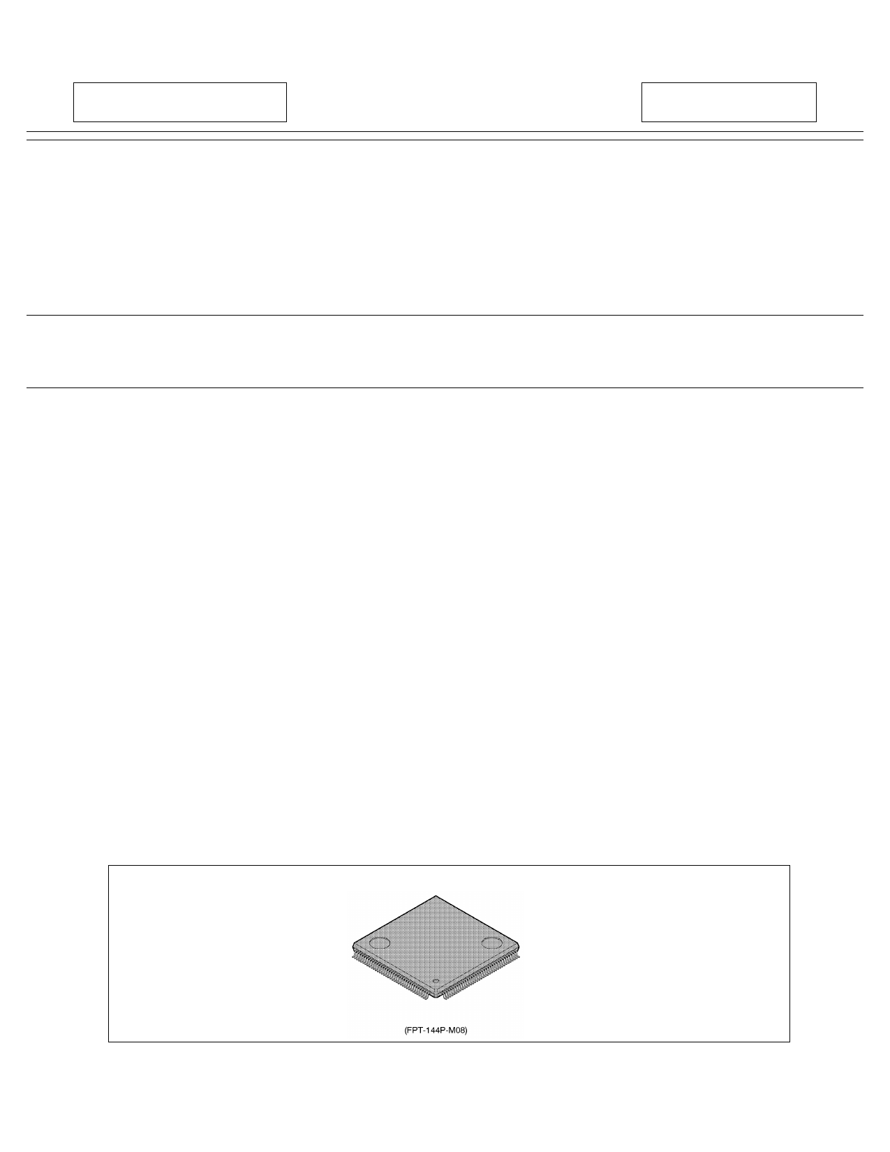
The device is fabricated by the advanced CMOS process and is housed in an 144-pin plastic Low profile shrink
Quad Flat Package (Suffix: –PMT).
s PACKAGE
144 Pin, Plastic LQFP
1 page 
• PCI Bus Interface Mode
(TOP VIEW)
AD23
V SS
AD22
AD21
AD20
V DD
AD19
V SS
AD18
AD17
AD16
V SS
C/BE2
FRAME
IRDY
V SS
TRDY
V DD
DEVSEL
STOP
V SS
PERR
PAR
C/BE1
V SS
AD15
AD14
AD13
AD12
V SS
V DD
AD11
AD10
AD9
V SS
AD8
1
5
10
15
20
25
30
35
INDEX
(FPT-144P-M08)
MB86605
LDBOEP
V DD
DB12
105 DB13
DB14
DB15
V SS
UDBP
100 DB0
DB1
V SS
DB2
DB3
95 DB4
DB5
V SS
DB6
DB7
90 LDBP
ATN
V SS
BSY
ACK
85 RST
MSG
SEL
V SS
C/D
80 REQ
I/O
DB8
V SS
DB9
75 DB10
DB11
V DD
5
5 Page 
MB86605
(Continued)
Pin no.
132
125
126
Pin name
DMBHE
(DMUDS)
DMA0
TP
(Transfer
permission)
I/O Function
I In 80-series mode: This is used to input the BHE signal output by
the DMAC when the upper byte of the DMA
data bus is valid.
In 68-series mode: This is used to input the UDS signal output by
the DMAC when the upper byte of the DMA
data bus is valid.
I This is used to input the address data A0 signal output by the
DMAC in the 80-series mode.
In 68-series mode: Connect to power supply pin (VDD).
I This is used to input DMA-transfer-enabling signals.
When the TP signal is active, the SPC performs the DMA transfer.
When this signal becomes inactive during DMA transfer, the
transfer stops temporarily at the block boundary.
4. PCI Bus Interface Mode
Pin no.
Pin name I/O
Function
130 PREQ
O This pin is used to request the bus arbiter for use of the bus.
129 GNT
I This is the response signal input pin to the REQ signal from the
bus arbiter.
132, 133, 135, 136, AD31 to AD0
138, 139, 141, 142,
1, 3 to 5, 7, 9 to 11,
26 to 29, 32 to 34, 36,
38, 39, 41, 42, 44,
46 to 48
I/O PCI 32-bit address and data multiplexed pins
143, 13, 24, 37 C/BE3 to C/BE0 I/O Bus command and Byte Enable signals multiplexed pins.
23 PAR
I/O This is an even parity signal pin for the AD31 to AD0 and C/BE3
to C/BE0 signals. This PAR signal becomes valid after one clock.
14
FRAME
I/O This is a frame signal pin that indicates data are transferring on
the bus.
17 TRDY
I/O Data Ready signal of Target side.
15 IRDY
I/O Data Ready signal of Initiator (Bus master) side.
20 STOP
I/O This is a stop request signal to stop the data transfer from target
to master.
19
DEVSEL
I/O Device select pin. While the device is a target, this pin outputs the
select signal that indicates the self device is selected. While the
device is a master this pin functions as an input pin to indicate
that a device on the bus is selected.
144 IDSEL
I This is a chip select signal that indicates the configuration access.
126 PCLK
I PCI bus clock input pin. The maximum clock frequency is 33
MHz.
22 PERR
I/O Data parity error input and output pin.
125 SERR
OD Address parity error output pin.
11
11 Page | ||
| Páginas | Total 30 Páginas | |
| PDF Descargar | [ Datasheet MB86605.PDF ] | |
Hoja de datos destacado
| Número de pieza | Descripción | Fabricantes |
| MB86603 | Communication Control Scsi-2 Protocol Controller | Fujitsu Microelectronics |
| MB86603 | (MB86603PFV) CMOS SCSI2 Protocol Controller | ETC |
| MB86604L | SCSI-II Protocol Controller (with single-ended driver/receiver) | Fujitsu Media Devices |
| MB86605 | Wide SCSI-II Protocol Controller | Fujitsu Media Devices |
| Número de pieza | Descripción | Fabricantes |
| SLA6805M | High Voltage 3 phase Motor Driver IC. |
Sanken |
| SDC1742 | 12- and 14-Bit Hybrid Synchro / Resolver-to-Digital Converters. |
Analog Devices |
|
DataSheet.es es una pagina web que funciona como un repositorio de manuales o hoja de datos de muchos de los productos más populares, |
| DataSheet.es | 2020 | Privacy Policy | Contacto | Buscar |