|
|
|
PDF 25L12835F Data sheet ( Hoja de datos )
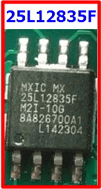
| Número de pieza | 25L12835F | |
| Descripción | MX25L12835F | |
| Fabricantes | Macronix | |
| Logotipo | ||
 1. serial Flash memory - MXIC Hay una vista previa y un enlace de descarga de 25L12835F (archivo pdf) en la parte inferior de esta página. Total 70 Páginas | ||
|
No Preview Available !
MX25L12835F
MX25L12835F
DATASHEET
P/N: PM1795
1 page 
MX25L12835F
• SI/SIO0
- Serial Data Input or Serial Data Input/Output for 2 x I/O read mode and 4 x I/O read mode
• SO/SIO1
- Serial Data Output or Serial Data Input/Output for 2 x I/O read mode and 4 x I/O read mode
• WP#/SIO2
- Hardware write protection or serial data Input/Output for 4 x I/O read mode
• RESET#/SIO3
- Hardware Reset pin or Serial input & Output for 4 x I/O read mode
• PACKAGE
-8-pin SOP (200mil)
-16-pin SOP (300mil)
-8-land WSON (6x5mm)
-8-land WSON (8x6mm)
- All devices are RoHS Compliant and Halogen-free
P/N: PM1795
REV. 1.3, OCT. 31, 2013
5
5 Page 
MX25L12835F
II. Additional 4K-bit secured OTP for unique identifier: to provide 4K-bit one-time program area for setting de-
vice unique serial number - Which may be set by factory or system customer.
- Security register bit 0 indicates whether the chip is locked by factory or not.
- To program the 4K-bit secured OTP by entering 4K-bit secured OTP mode (with Enter Security OTP command),
and going through normal program procedure, and then exiting 4K-bit secured OTP mode by writing Exit Security
OTP command.
- Customer may lock-down the customer lockable secured OTP by writing WRSCUR(write security register) com-
mand to set customer lock-down bit1 as "1". Please refer to Table 9. Security Register Definition for security reg-
ister bit definition and Table 3. 4K-bit Secured OTP Definition for address range definition.
- Note: Once lock-down whatever by factory or customer, it cannot be changed any more. While in 4K-bit secured
OTP mode, array access is not allowed.
Table 3. 4K-bit Secured OTP Definition
Address range
xxx000~xxx00F
xxx010~xxx1FF
Size
128-bit
3968-bit
Standard Factory Lock
ESN (electrical serial number)
N/A
Customer Lock
Determined by customer
P/N: PM1795
REV. 1.3, OCT. 31, 2013
11
11 Page | ||

| Páginas | Total 70 Páginas | |
| PDF Descargar | [ Datasheet 25L12835F.PDF ] | |
Hoja de datos destacado
| Número de pieza | Descripción | Fabricantes |
| 25L12835F | MX25L12835F | Macronix |
| Número de pieza | Descripción | Fabricantes |
| SLA6805M | High Voltage 3 phase Motor Driver IC. |
Sanken |
| SDC1742 | 12- and 14-Bit Hybrid Synchro / Resolver-to-Digital Converters. |
Analog Devices |
|
DataSheet.es es una pagina web que funciona como un repositorio de manuales o hoja de datos de muchos de los productos más populares, |
| DataSheet.es | 2020 | Privacy Policy | Contacto | Buscar |