|
|
|
PDF HC2509C Data sheet ( Hoja de datos )
| Número de pieza | HC2509C | |
| Descripción | Phase-Locked Loop Clock Distribution for Synchronous DRAM Applications | |
| Fabricantes | Hynix Semiconductor | |
| Logotipo | ||
Hay una vista previa y un enlace de descarga de HC2509C (archivo pdf) en la parte inferior de esta página. Total 6 Páginas | ||
|
No Preview Available !
HC2509C
March 1999
HC2509C
Features
l Phase-Locked Loop Clock Distribution for
Synchronous DRAM Applications
l Supports PC-100 and Meets “PC100 SDRAM
registered DIMM Specification Rev. 1.2”
l Distributes One Clock Input to One Bank of Five
and One Bank of Four Outputs
l No External RC Network Required
l External Feedback (FBIN) Pin is Used to
Synchronize the Outputs to the Clock Input
l Separate Output Enable for Each Output Bank
l Operates at 3.3 V Vcc
l 125 MHz Maximum Frequency
l On-chip Series Damping Resistors
l Support Spread Spectrum Clock(SSC)
Synthesizers
l ESD Protection Exceeds 3000 V per MIL-STD-
883, Method 3015 ; Exceeds 350 V Using
Machine Model ( C = 200 pF, R = 0 )
l Latch-Up Performance Exceeds 400 mA per
JESD 17
l Packaged in Plastic 24-Pin Thin Shrink Small-
Outline Package
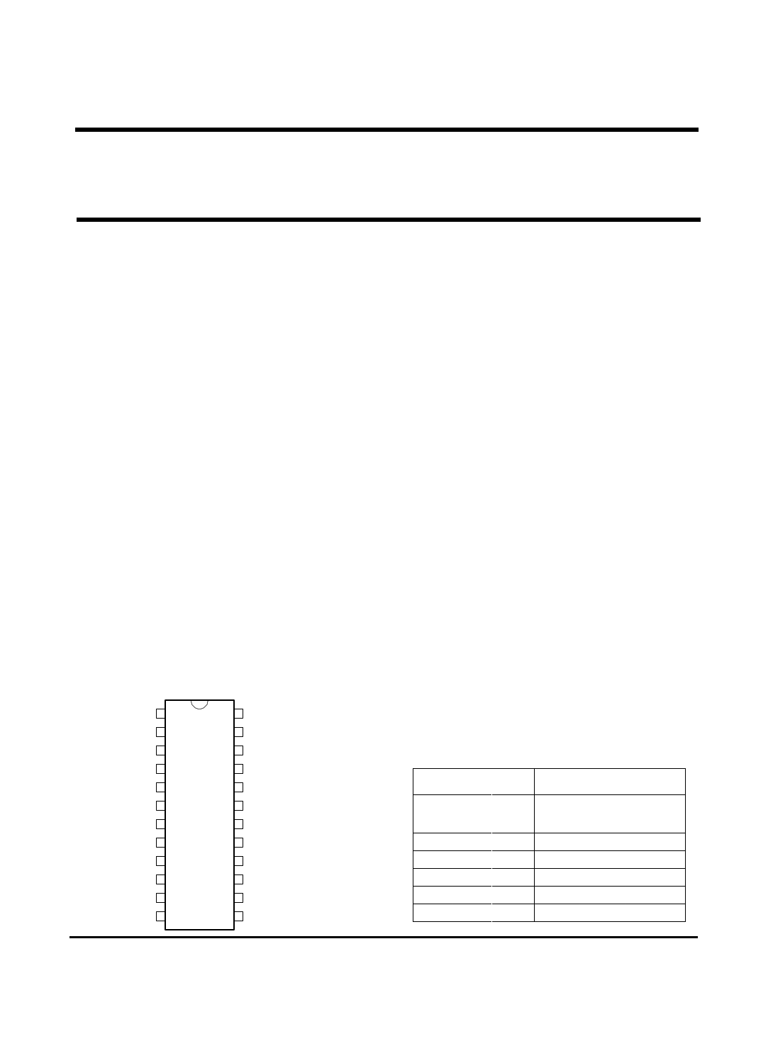
Pin Configuration
TSSOP 24 PACKAGE
(TOP VIEW)
AGND
Vcc
1Y0
1Y1
1Y2
GND
GND
1Y3
1Y4
Vcc
1G
FBOUT
1
2
3
4
5
6
7
8
9
10
11
12
24
23
22
21
20
19
18
17
16
15
14
13
CLK
AVcc
Vcc
2Y0
2Y1
GND
GND
2Y2
2Y3
Vcc
2G
FBIN
1
General Description
The HC2509C is a low-skew, low jitter, phase-locked
loop(PLL) clock driver, distributing high frequency
clock signals for SDRAM.
The HC2509C operates at 3.3V Vcc and provides
integrated series-damping resistors that make it ideal
for driving point-to-point loads. The propagation delay
from the CLK input to any clock output is nearly zero.
One bank of five outputs and one bank of four outputs
provide nine low-skew and low-jitter clocks. Each
bank of outputs can be enabled or disabled
separately via the control inputs (1G and 2G). Output
signal duty cycles are adjusted to 50 percent,
independent of the duty cycle at CLK.
The HC2509C is specially designed to interface with
high speed SDRAM applications in the range of
25MHz to 125MHz and includes an internal RC
network which provides excellent jitter characteristics
and eliminates the needs for external components.
For the test purpose, the PLL can be bypassed by
strapping AVcc to ground.
The HC2509C is characterized for operation from 0°C
to 85°C.
Function Table
INPUTS
1G 2G CLK
XX L
LLH
LHH
HL H
HHH
OUTPUTS
1Y
(0:4)
L
L
L
H
H
2Y
(0:3)
L
L
H
L
H
FBOUT
L
H
H
H
H
1 page 
HC2509C
March 1999
Table 6. Switching Characteristics Over Recommended Ranges of Supply
Voltage and Operating Free-air Temperature.(CL=30pF) (see Figure1 and 2) =
Parameter From(Input) TO(Output)
tphase error ♣
(normalized)
tsk
66MHz < CLKIN↑<
100MHz
CLKIN↑ = 100MHz
Any Y of FBOUT
Jitter(pk-pk)
CLKIN > 66MHz
Duty Cycle
tr
CLKIN > 66MHz
tf
=These parameters are not production tested.
♣ Phase error does not include jitter.
FBIN↑
FBIN↑
Any Y or
FBOUT
Any Y or
FBOUT
Any Y or
FBOUT
Any Y or
FBOUT
Any Y or
FBOUT
Vcc = 3.3V
Vcc =
±0.165V
3.3V±0.3V Unit
Min Typ Max Min Typ Max
-150
-150
ps
-50 50
ps
200 ps
-100
100 ps
45 55 %
1.3 1.9 0.8
2.1 ns
1.7 2.5 1.2
2.7 ns
Figure 1. Load Circuit and Voltage Waveforms
From Output Under Test
30pF
500§Ù
Load Circuit For Outputs
Input
tpd
50% Vcc
Output
0.4V
tr
2V
50% Vcc
tf
3V
2V
0.4V
0V
VOH
VOL
Voltage Waveforms
Propagation Delay Times
Notes: 1. All input pulses are supplied by generators having
the following characteristics: PRR ≤ 100MHz, Zo
=50Ω, tr =1.2ns, tf=1.2ns
2.The outputs are measured one at a time with one
transition per measurement.
5
5 Page | ||
| Páginas | Total 6 Páginas | |
| PDF Descargar | [ Datasheet HC2509C.PDF ] | |
Hoja de datos destacado
| Número de pieza | Descripción | Fabricantes |
| HC2509C | Phase-Locked Loop Clock Distribution for Synchronous DRAM Applications | Hynix Semiconductor |
| Número de pieza | Descripción | Fabricantes |
| SLA6805M | High Voltage 3 phase Motor Driver IC. |
Sanken |
| SDC1742 | 12- and 14-Bit Hybrid Synchro / Resolver-to-Digital Converters. |
Analog Devices |
|
DataSheet.es es una pagina web que funciona como un repositorio de manuales o hoja de datos de muchos de los productos más populares, |
| DataSheet.es | 2020 | Privacy Policy | Contacto | Buscar |