|
|
PDF ISL8126 Data sheet ( Hoja de datos )
| Número de pieza | ISL8126 | |
| Descripción | Dual/n-Phase Buck PWM Controller | |
| Fabricantes | Intersil | |
| Logotipo |  |
|
Hay una vista previa y un enlace de descarga de ISL8126 (archivo pdf) en la parte inferior de esta página. Total 30 Páginas | ||
|
No Preview Available !
DATASHEET
Dual/n-Phase Buck PWM Controller with Integrated
Drivers
ISL8126
The ISL8126 integrates two voltage-mode PWM leading-edge
modulation control with input feed-forward synchronous buck
PWM controllers to control dual independent voltage
regulators or a 2-phase single output regulator. It also
integrates current sharing control for the power module to
operate in parallel, which offers high system flexibility.
The ISL8126 integrates an internal linear regulator, which
generates IC’s bias voltages for applications with only one
single supply rail. The internal oscillator is adjustable from
150kHz to 1.5MHz, and is able to synchronize to an external
clock signal for frequency synchronization and phase
paralleling applications. Its PLL circuit can output a
phase-shift-programmable clock signal for the system to be
expanded to 3-, 4-, 6- and 12- phases with desired interleaving
phase shift.
The ISL8126’s Fault Spreading feature protects any channel
from overloading/stressing due to system faults or phase
failure. The undervoltage fault protection features are also
designed to prevent a negative transient on the output voltage
during falling down. This eliminates the Schottky diode that is
used in some systems for protecting the load device from
reversed output voltage damage.
Features
• Wide VIN range operation: 3V to 26.5V
- VCC operation from 3V to 5.60V
• Excellent output voltage regulation: 0.6V internal reference
• Frequency synchronization with programmable phase delay
up to 12-phase applications
• Fault spreading capability for high system reliability
• Digital soft-start with precharged output start-up capability
• Dual independent channel enable inputs with precision
voltage monitor and voltage feed-forward capability
- Programmable input voltage POR and its hysteresis with a
resistor divider at EN input
• Extensive circuit protection functions: output overvoltage,
undervoltage, overcurrent protection, over-temperature and
pre-power-on-reset overvoltage protection option
Applications
• Power supply for Datacom/Telecom and POL
• Paralleling power module
• Wide and narrow input voltage range buck regulators
Related Literature
• TB389 “PCB Land Pattern Design and Surface Mount
Guidelines for QFN Packages”
• AN1713, “ISL8126EVAL1Z Evaluation Board User Guide”
VO1
VIN
VO2
DUAL REGULATOR
0o VO
VIN
180o
TWO-PHASE REGULATOR
0o Vo 90o
180o
270o
FOUR-PHASE REGULATOR
FIGURE 1. TYPICAL APPLICATION DIAGRAM
January 29, 2015
FN7892.2
1
CAUTION: These devices are sensitive to electrostatic discharge; follow proper IC Handling Procedures.
1-888-INTERSIL or 1-888-468-3774 |Copyright Intersil Americas LLC 2011, 2012, 2015. All Rights Reserved
Intersil (and design) is a trademark owned by Intersil Corporation or one of its subsidiaries.
All other trademarks mentioned are the property of their respective owners.
1 page 
ISL8126
Functional Pin Descriptions (Continued)
PIN
NUMBER
29, 13
28, 14
27, 15
16
25, 17
24, 18
23, 19
22, 20
21
26
EPAD
SYMBOL
VSEN1+, VSEN2+
ISEN1B, ISEN2B
ISEN1A, ISEN2A
VIN
BOOT1, BOOT2
UGATE1, UGATE2
PHASE1, PHASE2
LGATE1, LGATE2
PVCC
VCC
GND
DESCRIPTION
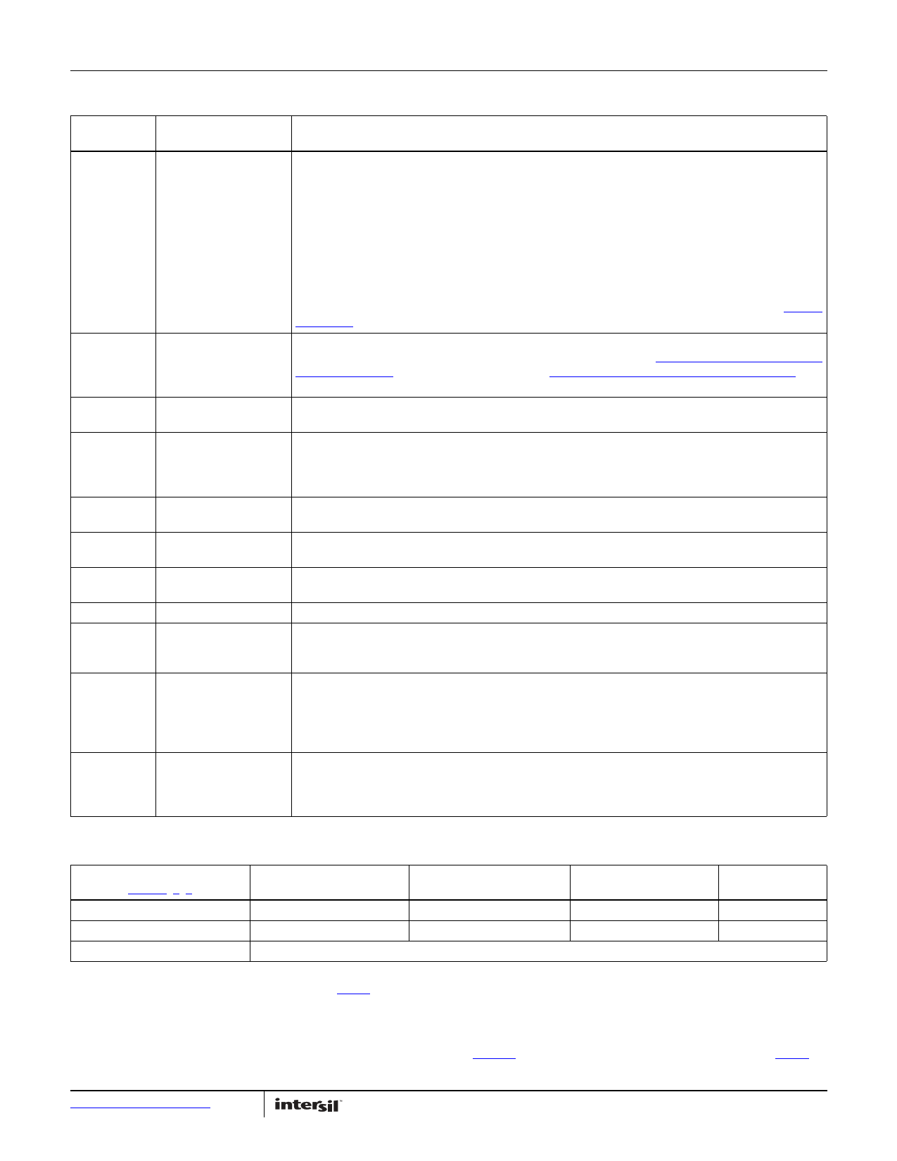
These pins are the positive inputs of the standard unity gain operational amplifier for differential remote
sense for the corresponding channel (Channels 1 and 2), and should be connected to the positive rail of the
load. These pins can also provide precision output voltage trimming capability by pulling a resistor from
this pin to the positive rail of the load (trimming down) or the return (typical VSEN1-, VSEN2- pins) of the
load (trimming up). By setting the resistor divider connected from the output voltage to the input of the
differential amplifier, the desired output voltage can be programmed. To minimize the system accuracy
error introduced by the input impedance of the differential amplifier, a resistor below 1kΩ is recommended
to be used for the lower leg (ROS) of the feedback resistor divider.
The typical input impedance of VSEN+ with respect to VSEN- is 500kΩ. With VSEN2- pulled within 400mV
of VCC, the corresponding error amplifier is disabled and VSEN2+ is one of the two pins to determine the
relative phase relationship between the internal clock of both channels and the CLKOUT signal. See Table 1
on page 23 for details.
These pins are the inverting (-) inputs of the current sensing amplifiers to provide rDS(ON), DCR, or precision
resistor current sensing together with the ISEN1A, ISEN2A pins. Refer to “2-Phase Operation with rDS(ON)
Sensing” on page 9 for rDS(ON) sensing set up and “2-Phase Operation with DCR Sensing” on page 8 for
DCR sensing set up.
These pins are the non-inverting (+) inputs of the current sensing amplifiers to provide rDS(ON), DCR, or
precision resistor current sensing together with the ISEN1B, ISEN2B pins.
This pin is the input of the internal linear regulator. It should be tied directly to the input rail. The internal
linear device is protected against reverse bias generated by the remaining charge of the decoupling
capacitor at PVCC when losing the input rail. When used with an external 3.3V to 5V supply, this pin can be
tied directly to PVCC to bypass the internal LDO.
These pins provide the bootstrap biases for the high-side drivers. Internal bootstrap diodes connected to
the PVCC pin provide the necessary bootstrap charge. Its typical operational voltage range is 2.5V to 5.6V.
These pins provide the gate signals to drive the high-side devices and should be connected to the MOSFETs’
gates.
Connect these pins to the source of the high-side MOSFETs and the drain of the low-side MOSFETs. These
pins represent the return path for the high-side gate drives.
These pins provide the drive for the low-side devices and should be connected to the MOSFETs’ gates.
This pin is the output of the internal series linear regulator. It provides the bias for both low-side and
high-side drives. Its operational voltage range is 3V to 5.6V. A 10µF ceramic capacitor is required for
decoupling PVCC to ground.
This pin provides bias power for the analog circuitry. An RC filter is recommended between the connection
of this pin to a 3V to 5.6V bias (typically PVCC). R is suggested to be a 5Ω resistor. And in 3.3V applications,
the R could be shorted to allow the low end input in concerns of the VCC falling threshold. The VCC
decoupling capacitor is strongly recommended to be a low ESR ceramic capacitor. This pin can be powered
either by the internal linear regulator or by an external voltage source.
The bottom pad is the signal and power ground plane. All voltage levels are referenced to this pad. This pad
provides a return path for the low-side MOSFET drives and internal power circuitries as well as all analog
signals. Connect this pad to the circuit ground with the shortest possible path (more than 5 to 6 vias to the
internal ground plane, placed on the soldering pad are recommended).
Ordering Information
PART NUMBER
(Notes 1, 2, 3)
PART MARKING
TEMP RANGE
(°C)
PACKAGE
(RoHS Compliant)
PKG.
DWG. #
ISL8126CRZ
ISL8126 CRZ
0 to +70
32 Ld 5x5 QFN
L32.5x5B
ISL8126IRZ
ISL8126 IRZ
-40 to +85
32 Ld 5x5 QFN
L32.5x5B
ISL8126EVAL1Z
Evaluation Board
NOTES:
1. Add “-T*” suffix for tape and reel. Please refer to TB347 for details on reel specifications.
2. These Intersil Pb-free plastic packaged products employ special Pb-free material sets, molding compounds/die attach materials, and 100% matte
tin plate plus anneal (e3 termination finish, which is RoHS compliant and compatible with both SnPb and Pb-free soldering operations). Intersil
Pb-free products are MSL classified at Pb-free peak reflow temperatures that meet or exceed the Pb-free requirements of IPC/JEDEC J STD-020.
3. For Moisture Sensitivity Level (MSL), please see device information page for ISL8126. For more information on MSL please see techbrief TB363.
Submit Document Feedback
5
FN7892.2
January 29, 2015
5 Page 
ISL8126
Typical Application Circuits (Continued)
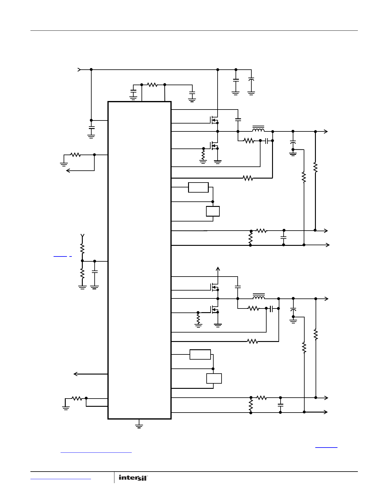
Double Data Rate I or II
+3.3 TO +26.5V
VIN
CF2
RCC
VCC
CF1
PVCC
BOOT1
VIN
CF3
UGATE1
PHASE1
CHFIN
CBIN
CBOOT1
Q1 LOUT1
RFS FSYNC
ISL8126
VDDQ
R*(VTT/0.6-1)
Note 4, 5)
R
CLKOUT/REFIN
1nF
(OR TIE REFIN PIN TO VMON1 PIN)
LGATE1
2kΩ
ISEN1A
ISEN1B
Q2
RISEN1
COMP1 ZCOMP1
FB1
VMON1
VSEN1+
VSEN1-
ZFB1
ROS1
RFB1
CSEN1
BOOT2
UGATE2
PHASE2
VDDQ Or VIN
CBOOT2
Q3 LOUT2
PGOOD
RSET
ISET
ISHARE
GND
LGATE2
ISEN2A
ISEN2B
2kΩ
COMP2 ZCOMP1
Q4
RISEN2
FB2
VMON2
VSEN2+
VSEN2-
ZFB1
ROS2
RFB2
CSEN2
2.5V (DDR I)
1.8V (DDR II)
VDDQ
COUT1
10Ω
10Ω
VSENSE1+
VSENSE1-
1.25V (DDR I)
0.9V (DDR II)
COUT2
VTT
( VDDQ/2)
10Ω
10
VSENSE2+
VSENSE2-
NOTES:
4. Setting the upper resistor to be a little higher than R*(VDDQ/0.7 - 1) will set the final REFIN voltage (stead state voltage after soft-start)
derived from the VDDQ to be a little higher than internal 0.6V reference. In this way, the VTT final voltage will use the internal 0.6V
reference after soft-start. The other way is to add more delay at EN/VFF1 pin to have Channel 2 tracking VDDQ (check the “DDR and
Dual Mode Operation” on page 36 for more details).
5. Another way to set REFIN voltage is to connect VMON1 directly to the REFIN pin.
Submit Document Feedback 11
FN7892.2
January 29, 2015
11 Page | ||
| Páginas | Total 30 Páginas | |
| PDF Descargar | [ Datasheet ISL8126.PDF ] | |
Hoja de datos destacado
| Número de pieza | Descripción | Fabricantes |
| ISL8120 | Dual/n-Phase Buck PWM Controller | Intersil Corporation |
| ISL8121 | Two-Phase Buck PWM Controller | Intersil Corporation |
| ISL8126 | Dual/n-Phase Buck PWM Controller | Intersil |
| ISL8126A | Dual/n-Phase Buck PWM Controller | Intersil |
| Número de pieza | Descripción | Fabricantes |
| SLA6805M | High Voltage 3 phase Motor Driver IC. |
Sanken |
| SDC1742 | 12- and 14-Bit Hybrid Synchro / Resolver-to-Digital Converters. |
Analog Devices |
|
DataSheet.es es una pagina web que funciona como un repositorio de manuales o hoja de datos de muchos de los productos más populares, |
| DataSheet.es | 2020 | Privacy Policy | Contacto | Buscar |
