|
|
|
PDF HCTS193MS Data sheet ( Hoja de datos )
| Número de pieza | HCTS193MS | |
| Descripción | Radiation Hardened Synchronous 4-Bit Up/Down Counter | |
| Fabricantes | Intersil Corporation | |
| Logotipo | ||
Hay una vista previa y un enlace de descarga de HCTS193MS (archivo pdf) en la parte inferior de esta página. Total 9 Páginas | ||
|
No Preview Available !
HCTS193MS
September 1995
Radiation Hardened
Synchronous 4-Bit Up/Down Counter
Features
Pinouts
• 3 Micron Radiation Hardened CMOS SOS
• Total Dose 200K RAD (Si)
• SEP Effective LET No Upsets: >100 MEV-cm2/mg
• Single Event Upset (SEU) Immunity < 2 x 10⁻⁹ Errors/Bit-
Day (Typ)
• Dose Rate Survivability: >1 x 10¹² RAD (Si)/s
• Dose Rate Upset >1010 RAD (Si)/s 20ns Pulse
• Latch-Up Free Under Any Conditions
• Fanout (Over Temperature Range)
- Standard Outputs - 10 LSTTL Loads
• Military Temperature Range: -55oC to +125oC
• Significant Power Reduction Compared to LSTTL ICs
• DC Operating Voltage Range: 4.5V to 5.5V
• LSTTL Input Compatibility
- VIL = 0.8V Max
- VIH = VCC/2 Min
• Input Current Levels Ii ≤ 5µA at VOL, VOH
Description
The Intersil HCTS193MS is a Radiation Hardened 4-bit binary
UP/DOWN synchronous counter.
Presetting the counter to the number on the preset data inputs
(P0 - P3) is accomplished by a low on the asynchronous parallel
load input (PL). The counter is incremented on the low to high
transition of the clock-up input (high on the clock-down),
decremented on the low to high transition of the clock-down input
(high on the clock-up). A high level on the MR input overrides any
other input to clear the counter to zero. The Terminal Count Up
goes low half a clock period before the zero count is reached and
returns high at the maximum count. The Terminal Count Down
mode goes low half a clock period before the maximum count
and returns high at the maximum count.
P1
Q1
Q0
CPD
CPU
Q2
Q3
GND
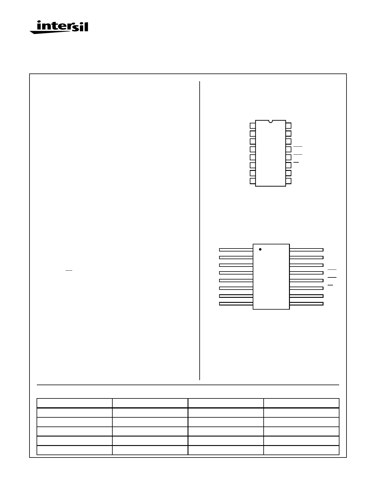
16 LEAD CERAMIC DUAL-IN-LINE
METAL SEAL PACKAGE (SBDIP)
MIL-STD-1835 CDIP2-T16
TOP VIEW
P1 1
Q1 2
Q0 3
CPD 4
CPU 5
Q2 6
Q3 7
GND 8
16 VCC
15 P0
14 MR
13 TCD
12 TCU
11 PL
10 P2
9 P3
16 LEAD CERAMIC METAL SEAL
FLATPACK PACKAGE (FLATPACK)
MIL-STD-1835 CDFP4-F16
TOP VIEW
1 16
2 15
3 14
4 13
5 12
6 11
7 10
89
The HCTS193MS utilizes advanced CMOS/SOS technology to
achieve high-speed operation. This device is a member of
radiation hardened, high-speed, CMOS/SOS Logic Family.
The HCTS193MS is supplied in a 16 lead Ceramic flatpack
(K suffix) or a SBDIP Package (D suffix).
VCC
P0
MR
TCD
TCU
PL
P2
P3
Ordering Information
PART NUMBER
HCTS193DMSR
HCTS193KMSR
HCTS193D/Sample
HCTS193K/Sample
HCTS193HMSR
TEMPERATURE RANGE
-55oC to +125oC
-55oC to +125oC
+25oC
+25oC
+25oC
SCREENING LEVEL
Intersil Class S Equivalent
Intersil Class S Equivalent
Sample
Sample
Die
CAUTION: These devices are sensitive to electrostatic discharge; follow proper IC Handling Procedures.
1-888-INTERSIL or 321-724-7143 | Copyright © Intersil Corporation 1999
592
PACKAGE
16 Lead SBDIP
16 Lead Ceramic Flatpack
16 Lead SBDIP
16 Lead Ceramic Flatpack
Die
Spec Number 518620
File Number 3066.1
1 page 
Specifications HCTS193MS
TABLE 3. ELECTRICAL PERFORMANCE CHARACTERISTICS (Continued)
LIMITS
PARAMETER
Pulse Width MR
SYMBOL
TW
CONDITIONS
VCC = 4.5V
Recovery Time
PL to CPU, CPD
Recovery Time
MR to CPU, CPD
TREC VCC = 4.5V
TREC VCC = 4.5V
NOTES
1
1
1
1
1
1
TEMPERATURE
+25oC
+125oC, 55oC
+25oC
+125oC, 55oC
+25oC
+125oC, 55oC
MIN MAX UNITS
20 - ns
30 - ns
15 - ns
22 - ns
5 - ns
5 - ns
NOTE:
1. The parameters listed in Table 3 are controlled via design or process parameters. Min and Max Limits are guaranteed but not directly
tested. These parameters are characterized upon initial design release and upon design changes which affect these characteristics.
TABLE 4. DC POST RADIATION ELECTRICAL PERFORMANCE CHARACTERISTICS
PARAMETER
Quiescent Current
Output Current (Sink)
Output Current
(Source)
Output Voltage Low
Output Voltage High
Input Leakage Current
Noise Immunity
Functional Test
CPU to Qn
CPD to Qn
PL to Qn
MR to Qn
SYMBOL
(NOTES 1, 2)
CONDITIONS
ICC VCC = 5.5V, VIN = VCC or GND
IOL VCC = 4.5V, VIN = VCC or GND,
VOUT = 0.4V
IOH VCC = 4.5V, VIN = VCC or GND,
VOUT = VCC -0.4V
VOL VCC = 4.5V or 5.5V, VIH = VCC/2,
VIL = 0.8V, IOL = 50µA
VOH
VCC = 4.5V or 5.5V, VIH = VCC/2,
VIL = 0.8V, IOL = -50µA
IIN VCC = 5.5V, VIN = VCC or GND
FN VCC = 4.5V, VIH = 2.25V, VIL = 0.8V,
(Note 3)
TPLH VCC = 4.5V
TPHL VCC = 4.5V
TPLH VCC = 4.5V
TPHL VCC = 4.5V
TPLH VCC = 4.5V
TPHL VCC = 4.5V
TPHL VCC = 4.5V
TEMPERATURE
+25oC
+25oC
200K RAD
LIMITS
MIN MAX UNITS
- 0.75 mA
4.0 - mA
+25oC
-4.0 - mA
+25oC
- 0.1 V
+25oC
+25oC
+25oC
VCC
-0.1
-
-
-
±5
-
V
µA
-
+25oC
+25oC
+25oC
+25oC
+25oC
+25oC
+25oC
2 34 ns
2 41 ns
2 36 ns
2 42 ns
2 36 ns
2 53 ns
2 44 ns
NOTES:
1. All voltages referenced to device GND.
2. AC measurements assume RL = 500Ω, CL = 50pF, Input TR = TF = 3ns, VIL = GND, VIH = 3V.
3. For functional tests VO ≥ 4.0V is recognized as a logic “1”, and VO ≤ 0.5V is recognized as a logic “0”.
Spec Number 518620
596
5 Page | ||
| Páginas | Total 9 Páginas | |
| PDF Descargar | [ Datasheet HCTS193MS.PDF ] | |
Hoja de datos destacado
| Número de pieza | Descripción | Fabricantes |
| HCTS193MS | Radiation Hardened Synchronous 4-Bit Up/Down Counter | Intersil Corporation |
| Número de pieza | Descripción | Fabricantes |
| SLA6805M | High Voltage 3 phase Motor Driver IC. |
Sanken |
| SDC1742 | 12- and 14-Bit Hybrid Synchro / Resolver-to-Digital Converters. |
Analog Devices |
|
DataSheet.es es una pagina web que funciona como un repositorio de manuales o hoja de datos de muchos de los productos más populares, |
| DataSheet.es | 2020 | Privacy Policy | Contacto | Buscar |