|
|
|
PDF LTC2668 Data sheet ( Hoja de datos )
| Número de pieza | LTC2668 | |
| Descripción | 16-Channel 16-/12-Bit DACs | |
| Fabricantes | Linear Technology | |
| Logotipo | ||
Hay una vista previa y un enlace de descarga de LTC2668 (archivo pdf) en la parte inferior de esta página. Total 26 Páginas | ||
|
No Preview Available !
Features
n Precision Reference 10ppm/°C Max
n Independently Programmable Output Ranges:
0V to 5V, 0V to 10V, ±2.5V, ±5V, ±10V
n Full 16-Bit/12-Bit Resolution at All Ranges
n Maximum INL Error: ±4LSB at 16 Bits
n A/B Toggle via Software or Dedicated Pin
n 16:1 Analog Multiplexer
n Guaranteed Monotonic Over Temperature
n Internal or External Reference
n Outputs Drive ±10mA Guaranteed
n 1.8V to 5V SPI Serial interface
n 6mm × 6mm 40-Lead QFN Package
Applications
n Optical Networking
n Instrumentation
n Data Acquisition
n Automatic Test Equipment
n Process Control and Industrial Automation
LTC2668
16-Channel 16-/12-Bit ±10V
VOUT SoftSpan DACs with
10ppm/°C Max Reference
Description
The LTC®2668 is a family of 16-channel, 16-/12-bit ±10V
digital-to-analog converters with integrated precision
references. They are guaranteed monotonic and have
built-in rail-to-rail output buffers. These SoftSpan™ DACs
offer five output ranges up to ±10V. The range of each
channel is independently programmable, or the part can
be hardware-configured for operation in a fixed range.
The integrated 2.5V reference is buffered separately to each
channel; an external reference can be used for additional
range options. The LTC2668 also includes A/B toggle
capability via a dedicated pin or software toggle command.
The SPI/Microwire-compatible 3-wire serial interface
operates on logic levels as low as 1.71V at clock rates
up to 50MHz.
L, LT, LTC, LTM, Linear Technology and the Linear logo are registered trademarks and
SoftSpan is a trademark of Linear Technology Corporation. All other trademarks are the property
of their respective owners.
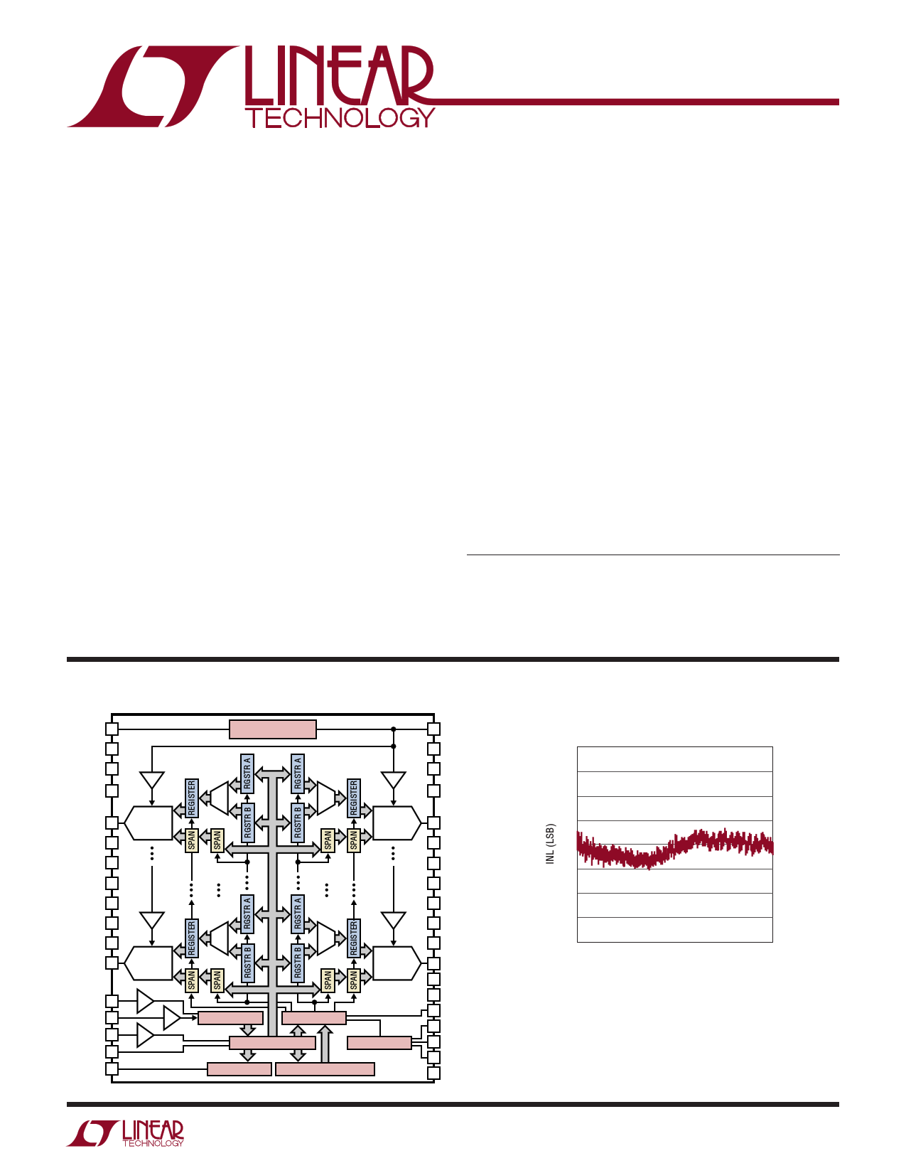
Block Diagram
REFCOMP 34
OVRTMP 38
GND
14, 37
REFLO
13, 35
VREF
VOUT0 2
VOUT1 3
VOUT2 4
VOUT3 5
VOUT4 6
VOUT5 7
VOUT6 8
VOUT7 9
DAC 0
VREF
DAC 7
CS/LD 16
SCK 17
SDI 19
SDO 18
MUX 12
INTERNAL REFERENCE
MUX MUX
VREF
33 REF
36 AVP
V+
10, 31
V–
11, 32
DAC 15
30 VOUT15
29 VOUT14
28 VOUT13
27 VOUT12
MUX
MUX
VREF
26 VOUT11
25 VOUT10
24 VOUT9
DAC 8
CONTROL LOGIC
DECODE
32-BIT SHIFT REGISTER
POWER-ON RESET
MONITOR MUX TOGGLE SELECT REGISTER
23 VOUT8
21 CLR
15 LDAC
20 TGP
39 MSP0
40 MSP1
1 MSP2
22 OVP
2668 TA01a
Integral Nonlinearity (LTC2668-16)
4
±10V RANGE
3
2
1
0
–1
–2
–3
–4
0
16384
32768
CODE
49152 65535
2668 TA01b
For more information www.linear.com/LTC2668
2668f
1
1 page 
LTC2668
E lectrical Characteristics The l denotes the specifications which apply over the full operating
temperature range, otherwise
unless otherwise specified.
specifications
are
at
TA
=
25°C.
AVP
=
5V,
OVP
=
5V,
V+
=
15V,
V
–
=
–15V,
VREF
=
2.5V,
VOUT
unloaded
SYMBOL PARAMETER
CONDITIONS
Reference Load Regulation
Reference Output Voltage Noise
Density
AVP = 5V ± 10%, IOUT = 100µA Sourcing
CREFCOMP = CREF = 0.1µF, at f = 10kHz
Reference Input Range
External Reference Mode (Note 8)
Reference Input Current
External Reference
Reference Input Capacitance (Note 9)
Power Supply
AVP Analog Supply Voltage
V+ Analog Positive Supply
V– Analog Negative Supply
V– Not Tied to GND
V– Tied to GND
OVP Digital I/O Supply Voltage
IAVP Supply Current AVP
AVP = 5V, Unipolar Ranges (Note 10)
AVP = 5V, Bipolar Ranges (Note 10)
IS Supply Current V+/V–
Unipolar Ranges (Code = 0)
Bipolar Ranges (Note 11)
IOVP Supply Current OVP (Note 12)
AVP Shutdown Supply Current
V+ Shutdown Supply Current
V– Shutdown Supply Current
OVP = 5V
OVP = AVP = 5V, V+/V– = ±15V
OVP = AVP = 5V, V+/V– = ±15V
OVP = AVP = 5V, V+/V– = ±15V
Monitor Mux
Monitor Mux DC Output Impedance
Monitor Mux Leakage Current
Monitor Mux Disabled (High Impedance)
Monitor Mux Output Voltage Range Monitor Mux Selected to DAC Channel
Monitor Mux Continuous Current
(Note 9)
AC Performance
tSET Settling Time (Notes 9, 13)
±0.024% (±1LSB at 12 Bits)
0V to 5V or ±2.5V Span, ±5V Step ±0.0015% (±1LSB at 16 Bits)
Settling Time (Notes 9, 13)
±0.024% (±1LSB at 12 Bits)
0V to 10V or ±5V Span, ±10V Step ±0.0015% (±1LSB at 16 Bits)
Settling Time (Notes 9, 13)
±10V Span, ±20V Step
±0.024% (±1LSB at 12 Bits)
±0.0015% (±1LSB at 16 Bits)
SR Voltage Output Slew Rate
Capacitive Load Driving
Glitch Impulse (Note 14)
At Mid-Scale Transition, 0V to 5V Range
DAC-to-DAC Crosstalk (Note 15) Due to Full-Scale Output Change
en Output Voltage Noise
0V to 5V Output Span,
Internal Reference
Density at f = 1kHz
Density at f = 10kHz
0.1Hz to 10Hz, Internal Reference
0.1Hz to 200kHz, Internal Reference
MIN
l 0.5
l
l
l 4.5
l 4.5
l –15.75
l –50
l 1.71
l
l
l
l
l
l
l
l –60
l
l V–
l
TYP MAX UNITS
140 mV/mA
32 nV/√Hz
0.001
40
AVP – 1.75
1
V
µA
pF
5.5
15.75
– 4.5
50
AVP + 0.3
5.4 6.5
9.4 12
4.6 6.5
8 9.5
0.02 1
13
35 70
–27
V
V
V
mV
V
mA
mA
mA
mA
µA
µA
µA
µA
2.2
0.02 1
V+ – 1.4
±1
kΩ
µA
V
mA
4.5 µs
9 µs
8 µs
9 µs
15.5 µs
20.5 µs
5 V/µs
1000 pF
3 nV • s
6 nV • s
90 nV/√Hz
80 nV/√Hz
1.7 µVRMS
55 µVRMS
For more information www.linear.com/LTC2668
2668f
5
5 Page 
LTC2668
Typical Performance Characteristics TA = 25°C, unless otherwise noted.
LTC2668-16/LTC2668-12
Mid-Scale Glitch Impulse
DAC-to-DAC Crosstalk
CS/LD
VOUT
10mV/DIV
3nV-s TYP
OV+V,PV,–A:V±P1:55VV
0V TO 5V RANGE
INTERNAL REFERENCE
CREF, CREFCOMP: 0.1µF
CS/LD
6nV-s TYP
VOUT
10mV/DIV
1µs/DIV
2668 G28
FALLING MAJOR CARRY TRANSITION
RISING TRANSITION IS SIMILAR OR BETTER
ALL CHANNELS ARE SIMILAR OR BETTER
1µs/DIV
2668 G29
OVP, AVP: 5V
V+, V–: ±15V
0V TO 10V RANGE
INTERNAL REFERENCE
CREF, CREFCOMP: 0.1µF
SUBJECT CHANNEL: VOUT0
AGGRESSOR CHANNEL:
VOUT1 10V TO 0V STEP
VOUT1 RISING IS SIMILAR OR BETTER
ALL CHANNELS ARE SIMILAR OR BETTER
Large Signal Response
15
0V TO 10V RANGE
10
5
0V TO 5V RANGE
0
–5
±10V RANGE
–10
–15
10µs/DIV
2668 G30
Noise Density vs Frequency
500
Output 0.1Hz to 10Hz Voltage
Noise
400
300
VOUT
10µV/DIV
200
100
0
10 100 1k 10k 100k 1M
FREQUENCY (Hz)
2668 G31
1s/DIV
AVP = 5V, V+, V– = ±15V
0V TO 5V RANGE
CODE = MID-SCALE
INTERNAL REFERENCE
CREF = CREFCOMP = 0.1µF
2668 G32
Reference 0.1Hz to 10Hz
Voltage Noise
VREF
10µV/DIV
1s/DIV
AVP = 5V, V+, V– = ±15V
VREF = 2.5V
CREF = CREFCOMP = 0.1µF
2668 G33
Load Regulation
10
8
78µV/mA TYP
CODE: MID-SCALE
6 INTERNAL REF
4
2
0
–2
–4
–6
–8
–10
–30
0AVVPT,OV5+V=R5AVN, VG–E,= GND
±A1V0PV=R5AVN, GVE+,/V– = ±15V
–20 –10 0 10 20 30
VOUT LOAD CURRENT (mA)
40
2668 G34
For more information www.linear.com/LTC2668
2668f
11
11 Page | ||
| Páginas | Total 26 Páginas | |
| PDF Descargar | [ Datasheet LTC2668.PDF ] | |
Hoja de datos destacado
| Número de pieza | Descripción | Fabricantes |
| LTC2664 | SoftSpan DACs | Linear Technology |
| LTC2668 | 16-Channel 16-/12-Bit DACs | Linear Technology |
| Número de pieza | Descripción | Fabricantes |
| SLA6805M | High Voltage 3 phase Motor Driver IC. |
Sanken |
| SDC1742 | 12- and 14-Bit Hybrid Synchro / Resolver-to-Digital Converters. |
Analog Devices |
|
DataSheet.es es una pagina web que funciona como un repositorio de manuales o hoja de datos de muchos de los productos más populares, |
| DataSheet.es | 2020 | Privacy Policy | Contacto | Buscar |