|
|
|
PDF LTC2960 Data sheet ( Hoja de datos )
| Número de pieza | LTC2960 | |
| Descripción | 36V Nano-Current Two Input Voltage Monitor | |
| Fabricantes | Linear Technology | |
| Logotipo | ||
1. LTC2960 Hay una vista previa y un enlace de descarga de LTC2960 (archivo pdf) en la parte inferior de esta página. Total 16 Páginas | ||
|
No Preview Available !
FEATURES
n 850nA Quiescent Current
n Operating Range: 2.5V < VCC < 36V
n 1.5% (Max) Accuracy Over Temperature
n Adjustable Reset Threshold
n Wide Temperature Range (–40°C to 125°C)
n Adjustable IN+/IN– Threshold
n Manual Reset Input
n Compact 2mm × 2mm 8-lead DFN and
TSOT-23 (ThinSOT™) Packages
APPLICATIONS
n Portable Equipment
n Battery Powered Equipment
n Security Systems
n Automotive Systems
LTC2960 Option Table
Option
LTC2960-1
LTC2960-2
LTC2960-3
LTC2960-4
Inputs
ADJ/IN+
ADJ/IN–
ADJ/IN+
ADJ/IN–
Reset Timeout Period
15ms/200ms
15ms/200ms
200ms
200ms
Output Type
36V Open-Drain
36V Open-Drain
Active Pull-up
Active Pull-up
LTC2960
36V Nano-Current
Two Input Voltage Monitor
DESCRIPTION
The LTC®2960 is a nano-current, high voltage two input
voltage monitor, ideally suited for multicell battery ap-
plications. External resistive dividers configure custom
comparator thresholds. The supervisory circuit monitors
the ADJ input and pulls the RST output low when the input
drops below threshold. A reset timeout period delays the
return of the RST output to a high state when the input
rises above the threshold. The spare comparator allows
voltage conditions to be detected with either a non-inverting
input, IN+(LTC2960-1/LTC2960-3) or an inverting input,
IN– (LTC2960-2/LTC2960-4). A manual reset (MR) input
is provided for external activation of the reset output.
Other options provided on the LTC2960-1/LTC2960-2 in-
clude a reset timeout period select pin, RT, to select between
15ms or 200ms reset timeout periods. The LTC2960-3/
LTC2960-4 have a fixed 200ms reset timeout period. The
RST and OUT outputs are available with active pull-up cir-
cuits to an output logic supply pin (LTC2960-3/LTC2960-4)
or 36V open-drain outputs (LTC2960-1/LTC2960-2).
L, LT, LTC, LTM, Linear Technology and the Linear logo are registered trademarks and
ThinSOT is a trademark of Linear Technology Corporation. All other trademarks are the property
of their respective owners.
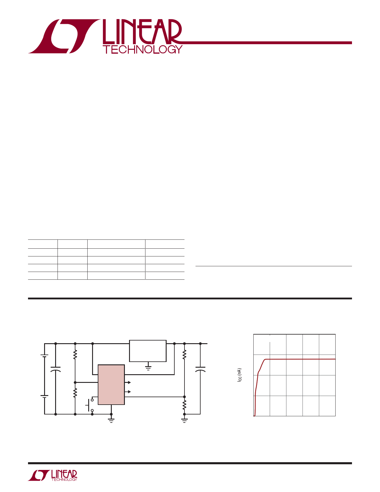
TYPICAL APPLICATION
Battery and Regulator Monitor
6V < VIN < 8.4V
Li-Ion +
4.2V
C1
0.1μF
50V
R2
6.04M
Li-Ion +
4.2V
R1
402k
LTC2960-3
VCC DVCC
IN+ RST
OUT
MR ADJ
GND
LTC3632
DC/DC
GND
RESET
LOW BATTERY
POWER-FAIL FALLING THRESHOLD = 6.410V
RESET FALLING THRESHOLD = 1.693V
R4
1.3M
VOUT
1.8V
C2
1μF
R3
402k
2960 TA01
Supply Current vs Supply Voltage
1200
MR=5V, 27C
900
600
300
0
0 8 16 24 32 40
VCC (V)
2960 TA01a
2960f
1
1 page 
TYPICAL PERFORMANCE CHARACTERISTICS
LTC2960
MR Rising Threshold/Open
Voltage vs VCC
2.4
MR OPEN VOLTAGE 27°C
1.9
1.4
MR INPUT THRESHOLD 27°C
0.9
Normalized Reset Timeout Period
vs Temperature
1.3
VCC = 7V
1.2
1.1
1.0
0.9
0.8
Comparator Overvoltage/
Undervoltage Glitch Immunity
4.0 ADJ/IN+/IN–
VCC = 7V
3.0
2.0
1.0
0.4
2.5
3.0 3.5 4.0 4.5 5.0
VCC (V)
2960 G04
0.7
–50 –25
0 25 50 75
TEMPERATURE (°C)
100 125
2960 G05
0.0
0.1
1 10
COMPARATOR OVERDRIVE (%)
100
2960 G06
ADJ, IN+, IN– Threshold
vs Temperature
430
V+HYS
420
VRHYS
410
VTH
400
390
V–HYS
380
370
–50 –25
0 25 50 75
TEMPERATURE (°C)
100 125
2960 G07
Voltage Output HIGH vs
Pull-Down Current (RST/OUT)
3.5
125°C
3.0
90°C
27°C
–45°C
2.5
2.0
1.5
1.0
0.5 VCC =7V
DVCC =3.3V
0
0 –0.2 –0.4 –0.6
PULL-DOWN CURRENT(mA)
–0.8
2960 G08
Voltage Output LOW vs
Pull-Up Current (RST/OUT)
2.0
125°C
90°C
1.6
27°C
–45°C
Voltage Output HIGH vs
Pull-Down Current (RST/OUT)
2.0
125°C
90°C
1.6
27°C
–45°C
1.2 1.2
0.8 0.8
0.4
0
0
VCC =7V
DVCC =3.3V
1234
PULL-UP CURRENT (mA)
5
2960 G09
0.4
VCC =7V
DVCC =1.6V
0
0 –20 –40 –60
PULL-DOWN CURRENT(μA)
–80
2960 G08
2960f
5
5 Page 
LTC2960
APPLICATIONS INFORMATION
VA
R4
681k
VB
LTC2960-3
DVCC
R5
48.7k
IN+ OUT
R6
6.81M
2960 F06
Figure 6. External Hysteresis
The addition of R6 allows OUT to sink or source current
to the summing junction at IN+. Neglecting internal switch
resistances and providing that R6 >> R5, the externally
modified hysteresis (referred to VA) becomes:
VHEXT
≈
VH YS( VA )
+
VB
⎛⎝⎜
R4
R6
⎞⎠⎟
Since the amount of hysteresis is to be doubled, the
second term in the above expression needs to be about
300mV. With a logic supply, VB, equal to 3V, the ratio R4/
R6 should be about 0.1. Choosing R6 to be 6.81M satis-
fies the design criteria.
The addition of R6 modifies the rising and falling thresholds
originally determined by R4 and R5. The modified rising
threshold becomes:
( )VR=
VTH + V+HYS
•
⎛
⎜1+
R
4
+
R4
⎞
⎟
⎝ R5 R6 ⎠
= (400mV + 20mV) • (1+ 13.98 + 0.1)
= 6.3336V
It is apparent that the R4/R6 term does not affect the ris-
ing threshold significantly resulting in a change of only
+0.645%. The falling threshold incorporating R6 is:
VF
=
VTH
⎛
⎝⎜ 1+
R4
R5
+
R4 ⎛
R6 ⎝⎜
VTH – VB
VTH
⎞⎞
⎠⎟ ⎠⎟
= 0.4V • (1+ 13.98 – 0.65) = 5.732V
The falling threshold can be restored to the original value
by reducing the value of R5. Under the assumption that
the addition of R6 has a negligible impact on the rising
threshold, a new R4/R5 ratio can be calculated as shown:
( )R4 =
R5
VR
VTH + V+HYS
– 1= 6.6V – 1= 14.71
420mV
Given the ratio of R4/R5, the closest 1% resistor value for
R5 is 46.4k. With the actual resistor values now known,
the final thresholds can be calculated by plugging the
values into the equations above for VR and VF to obtain:
VR = 6.626V, VF = 6.010V, VHYST = 616mV
As a result of the added current component through R6
an error term exists that is a function of the pull-up volt-
age, VB in Figure 6.
Operation with Supply Transients over 40V and Hot
Swapping
The circuit in Figure 7(a) allows the LTC2960 to withstand
high voltage transients. The magnitude of the voltage
transients that can be absorbed is set by the voltage rat-
ing of RZ. A TT-IRC pulse-withstanding surface mount
1206 resistor with a nominal voltage rating of 200V is
used. The external 30V Zener diode (Z1) and the 143kΩ
current limiting resistor (RZ) protect the VIN supply pin
of the LTC2960. Note that there is a speed penalty which
is the time constant determined by RZ and C1, 14.3ms in
this example. If VIN is below 30V, there is a voltage drop
across RZ that is dependent on the quiescent current of
the LTC2960 which is nominally less than 150mV but can
be as high as 290mV if MR is pulled low. The maximum
voltage drop is determined by the maximum specified ICC
and MR pull-up currents. For conditions where the Zener
conducts current, it can be biased in the microamp range
owing to the low quiescent current of the LTC2960. For a
supply voltage of 150V, the Zener is biased <1mA. When
input pins are used to sense VIN, the input pins ADJ/IN+/
IN– absolutemaximumratingof3.5Vmustnotbeexceeded.
VIN can be a maximum of 8.75x the lowest programmed
threshold to satisfy this condition. For a maximum VIN of
150V, the lowest programmable threshold is >17V.
2960f
11
11 Page | ||
| Páginas | Total 16 Páginas | |
| PDF Descargar | [ Datasheet LTC2960.PDF ] | |
Hoja de datos destacado
| Número de pieza | Descripción | Fabricantes |
| LTC2960 | 36V Nano-Current Two Input Voltage Monitor | Linear Technology |
| LTC2965 | 100V Micropower Single Voltage Monitor | Linear |
| Número de pieza | Descripción | Fabricantes |
| SLA6805M | High Voltage 3 phase Motor Driver IC. |
Sanken |
| SDC1742 | 12- and 14-Bit Hybrid Synchro / Resolver-to-Digital Converters. |
Analog Devices |
|
DataSheet.es es una pagina web que funciona como un repositorio de manuales o hoja de datos de muchos de los productos más populares, |
| DataSheet.es | 2020 | Privacy Policy | Contacto | Buscar |