|
|
PDF IS43R16320D Data sheet ( Hoja de datos )
| Número de pieza | IS43R16320D | |
| Descripción | 16Mx32 32Mx16 64Mx8 512Mb DDR SDRAM | |
| Fabricantes | Integrated Silicon Solution | |
| Logotipo | ||
Hay una vista previa y un enlace de descarga de IS43R16320D (archivo pdf) en la parte inferior de esta página. Total 30 Páginas | ||
|
No Preview Available !
IS43/46R86400D
IS43/46R16320D, IS43/46R32160D
16Mx32, 32Mx16, 64Mx8 NOVEMBER 2012
512Mb DDR SDRAM
FEATURES
• VDD and VDDQ: 2.5V ± 0.2V (-6)
• VDD and VDDQ: 2.6V ± 0.1V (-5)
• SSTL_2 compatible I/O
• Double-data rate architecture; two data transfers
per clock cycle
• Bidirectional, data strobe (DQS) is transmitted/
received with data, to be used in capturing data
at the receiver
• DQS is edge-aligned with data for READs and
centre-aligned with data for WRITEs
• Differential clock inputs (CK and CK)
• DLL aligns DQ and DQS transitions with CK
transitions
• Commands entered on each positive CK edge;
data and data mask referenced to both edges of
DQS
• Four internal banks for concurrent operation
• Data Mask for write data. DM masks write data
at both rising and falling edges of data strobe
• Burst Length: 2, 4 and 8
• Burst Type: Sequential and Interleave mode
• Programmable CAS latency: 2, 2.5 and 3
• Auto Refresh and Self Refresh Modes
• Auto Precharge
• TRAS Lockout Supported (tRAP = tRCD )
OPTIONS
• Configuration(s): 16Mx32, 32Mx16, and 64Mx8
• Package(s): 144 Ball BGA (x32), 66-pin TSOP-II
(x8, x16), and 60 Ball BGA (x8, x16)
• Lead-free package
• Temperature Range:
Commercial (0°C to +70°C)
Industrial (-40°C to +85°C)
Automotive, A1 (-40°C to +85°C)
Automotive, A2 (-40°C to +105°C)
DEVICE OVERVIEW
ISSI’s 512-Mbit DDR SDRAM achieves high speed data
transfer using pipeline architecture and two data word
accesses per clock cycle. The 536,870,912-bit memory
array is internally organized as four banks of 128Mb to
allow concurrent operations. The pipeline allows Read
and Write burst accesses to be virtually continuous, with
the option to concatenate or truncate the bursts. The
programmable features of burst length, burst sequence
and CAS latency enable further advantages. The device
is available in 8-bit, 16-bit and 32-bit data word size
Input data is registered on the I/O pins on both edges
of Data Strobe signal(s), while output data is referenced
to both edges of Data Strobe and both edges of CLK.
Commands are registered on the positive edges of CLK.
An Auto Refresh mode is provided, along with a Self
Refresh mode. All I/Os are SSTL_2 compatible.
ADDRESS TABLE
Parameter 16M x 32
Configuration 4M x 32 x 4
banks
Bank Address BA0, BA1
Pins
Autoprecharge A8/AP
Pins
Row Address 8K(A0 – A12)
Column
Address
512(A0 – A7,
A9)
Refresh Count
Com./Ind./A1 8K / 64ms
A2 8K / 16ms
32M x 16
8M x 16 x 4
banks
BA0, BA1
A10/AP
8K(A0 – A12)
1K(A0 – A9)
8K / 64ms
8K / 16ms
64M x 8
16M x 8 x 4
banks
BA0, BA1
A10/AP
8K(A0 – A12)
2K(A0 – A9,
A11)
8K / 64ms
8K / 16ms
KEY TIMING PARAMETERS
Speed Grade
-5 -6
Fck Max CL = 3 200 167
Fck Max CL = 2.5 167 167
Fck Max CL = 2 133 133
Units
MHz
MHz
MHz
Copyright © 2012 Integrated Silicon Solution, Inc. All rights reserved. ISSI reserves the right to make changes to this specification and its products at any time without
notice. ISSI assumes no liability arising out of the application or use of any information, products or services described herein. Customers are advised to obtain the
latest version of this device specification before relying on any published information and before placing orders for products.
Integrated Silicon Solution, Inc. does not recommend the use of any of its products in life support applications where the failure or malfunction of the product can rea-
sonably be expected to cause failure of the life support system or to significantly affect its safety or effectiveness. Products are not authorized for use in such applica-
tions unless Integrated Silicon Solution, Inc. receives written assurance to its satisfaction, that:
a.) the risk of injury or damage has been minimized;
b.) the user assume all such risks; and
c.) potential liability of Integrated Silicon Solution, Inc is adequately protected under the circumstances
Integrated Silicon Solution, Inc. 1
Rev.C
11/20/2012
1 page 
IS43/46R86400D
IS43/46R16320D, IS43/46R32160D
PIN CONFIGURATION
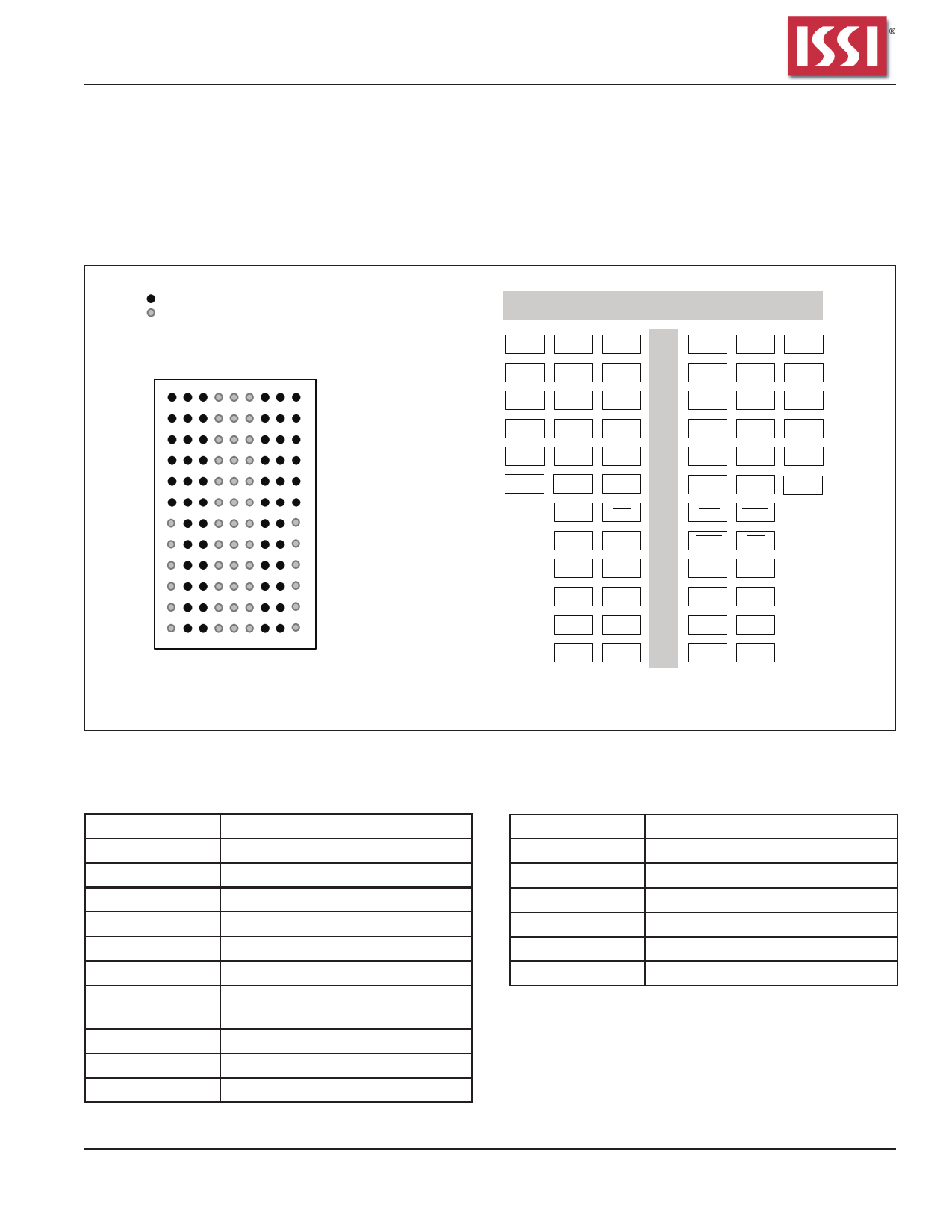
Package Code B: 60-ball FBGA (top view) for x8
(8mm x 13mm Body, 0.8mm Ball Pitch)
Top View
(Balls seen through the Package)
: Ball Existing
: Depopulated Ball
Top View(See the balls through the Package)
1 23456789
A
B
C
D
E
F
G
H
J
K
L
M
BGA Package Ball Pattern
Top View
1 23
78
9
VSSQ DQ7 VSS A VDD DQ0 VDDQ
NC VDDQ DQ6 B DQ1 VSSQ NC
NC VSSQ DQ5 C DQ2 VDDQ NC
NC VDDQ DQ4 D DQ3 VSSQ NC
NC VSSQ
VREF VSS
DQS
DM
E
F
NC VDDQ NC
NC VDD NC
CK CK G WE CAS
A12 CKE H RAS CS
A11 A9 J BA1 BA0
A8 A7 K A0 A10/AP
A6 A5 L A2 A1
A4 VSS M VDD A3
x 8 Device Ball Pattern
PIN DESCRIPTION: x8
A0-A12
A0-A9, A11
BA0, BA1
DQ0 – DQ7
CK, CK
CKE
CS
CAS
RAS
WE
DM
Row Address Input
Column Address Input
Bank Select Address
Data I/O
System Clock Input
Clock Enable
Chip Select
Column Address Strobe
Command
Row Address Strobe Command
Write Enable
Data Write Mask
Integrated Silicon Solution, Inc.
Rev. C
11/20/2012
DQS
VDD
VDDQ
VSS
VSSQ
VREF
NC
Data Strobe
Power
Power Supply for I/O Pins
Ground
Ground for I/O Pins
SSTL_2 reference voltage
No Connection
5
5 Page 
IS43/46R86400D
IS43/46R16320D, IS43/46R32160D
TRUTH TABLE - CKE
CKE n-1
L
L
L
L
H
H
H
H
CKE n
L
L
H
H
L
L
L
H
Current State
Power Down
Self Refresh
Power Down
Self Refresh
All Banks Idle
Bank(s) Active
All Banks Idle
COMMAND n
ACTION n
X Maintain Power Down
X Maintain Self Refresh
NOP or DESELECT Exit Power Down
NOP or DESELECT Exit Self Refresh
NOP or DESELECT Precharge Power Down Entry
NOP or DESELECT Active Power Down Entry
AUTO REFRESH
Self Refresh entry
See Truth Tables - Commands
NOTES
6
6, 7
6
6
Notes:
1. CKEn is the logic state of CKE at clock edge n; CKEn-1 was the state of CKE at the previous clock edge.
2. Current state is the state of DDR immediately prior to clock edge n.
3. COMMANDn is the command registered at clock edge n, and ACTIONn is the result of COMMANDn.
4. All states and sequences not shown are illegal or reserved.
5. CKE must not go LOW during a Read or Write, and must stay HIGH until after trpst or twr, respectively.
6. DESELECT and NOP are functionally interchangeable.
7. NOPs or Deselects must be issued for at least tsnr after Self-Refresh exit before any other command. After DLL Reset, at
least txsrd must elapse before any Read commands occur.
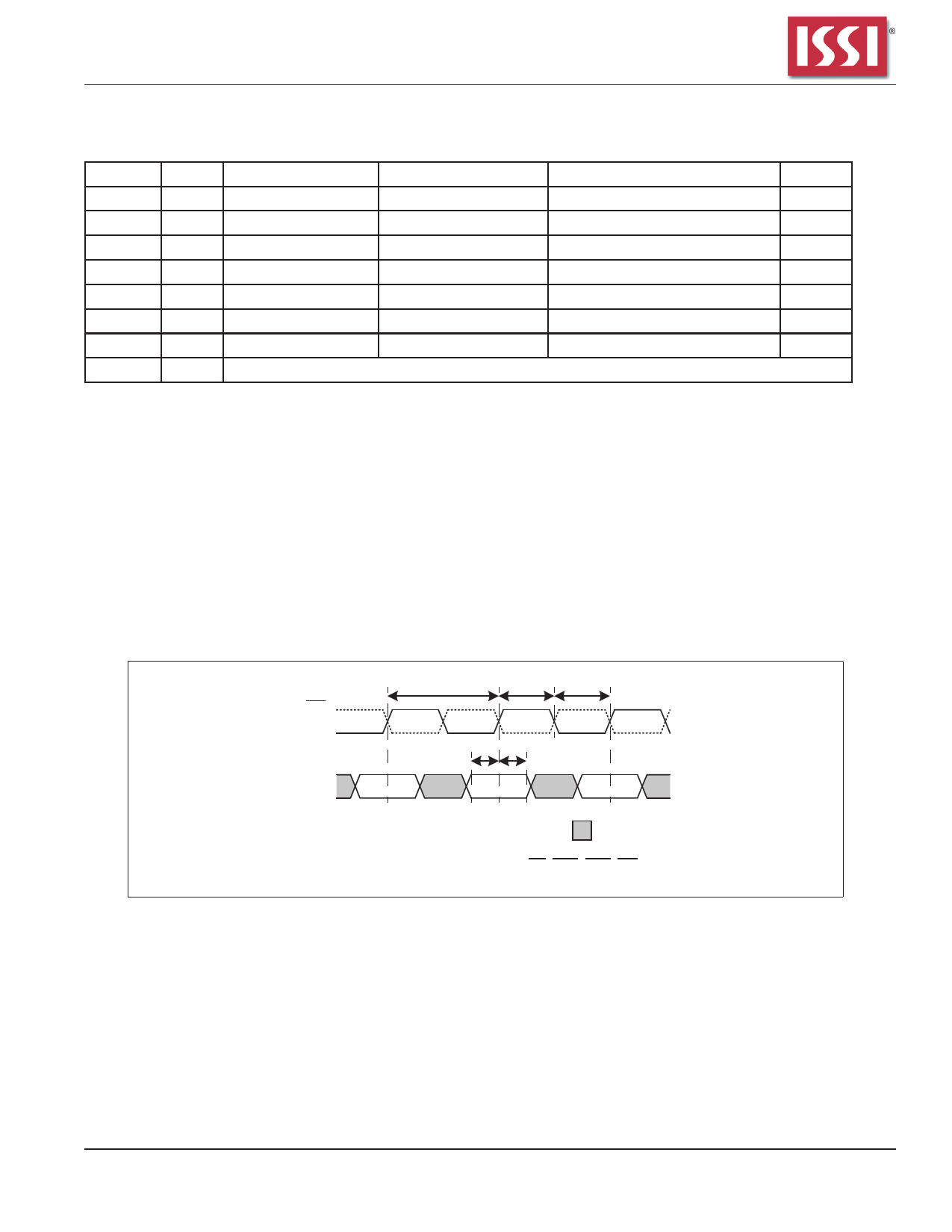
Basic Timing Parameters for Commands
CK
CK
Input
tCK tCH tCL
Valid
tIS tIH
Valid
Valid
= Don't Care
NOTE: Input = A0 - An, BA0, BA1, CKE, CS, RAS, CAS, WE;
An = Address bus MSB
Integrated Silicon Solution, Inc. 11
Rev. C
11/20/2012
11 Page | ||
| Páginas | Total 30 Páginas | |
| PDF Descargar | [ Datasheet IS43R16320D.PDF ] | |
Hoja de datos destacado
| Número de pieza | Descripción | Fabricantes |
| IS43R16320A | 32Meg x 16 512-MBIT DDR SDRAM | Integrated Silicon Solution |
| IS43R16320D | 16Mx32 32Mx16 64Mx8 512Mb DDR SDRAM | Integrated Silicon Solution |
| IS43R16320E | 512Mb DDR SDRAM | Integrated Silicon Solution |
| Número de pieza | Descripción | Fabricantes |
| SLA6805M | High Voltage 3 phase Motor Driver IC. |
Sanken |
| SDC1742 | 12- and 14-Bit Hybrid Synchro / Resolver-to-Digital Converters. |
Analog Devices |
|
DataSheet.es es una pagina web que funciona como un repositorio de manuales o hoja de datos de muchos de los productos más populares, |
| DataSheet.es | 2020 | Privacy Policy | Contacto | Buscar |
