|
|
|
PDF HCPL-0701 Data sheet ( Hoja de datos )
| Número de pieza | HCPL-0701 | |
| Descripción | Low Input Current/ High Gain Optocouplers | |
| Fabricantes | Agilent(Hewlett-Packard) | |
| Logotipo | ||
Hay una vista previa y un enlace de descarga de HCPL-0701 (archivo pdf) en la parte inferior de esta página. Total 16 Páginas | ||
|
No Preview Available !
Low Input Current, High Gain
Optocouplers
Technical Data
6N139
6N138
HCPL-0701 HCPL-0700
HCNW139 HCNW138
Features
• High Current Transfer Ratio
– 2000% Typical (4500%
Typical for HCNW139/138)
• Low Input Current
Requirements – 0.5 mA
• TTL Compatible Output –
0.1 V VOL Typical
• Performance Guaranteed
over Temperature 0°C
to 70°C
• Base Access Allows Gain
Bandwidth Adjustment
• High Output Current –
60 mA
• Safety Approval
UL Recognized – 2500 V rms
for 1 Minute and 5000 V rms*
for 1 Minute per UL 1577
CSA Approved
VDE 0884 Approved with
VIORM = 1414 V peak for
HCNW139 and HCNW138
BSI Certified (HCNW139 and
HCNW138)
• Available in 8-Pin DIP or
SOIC-8 Footprint or
Widebody Package
•MIL-STD-1772 Version
Available (HCPL-5700/1)
Applications
• Ground Isolate Most Logic
Families – TTL/TTL, CMOS/
TTL, CMOS/CMOS, LSTTL/
TTL, CMOS/LSTTL
• Low Input Current Line
Receiver
• High Voltage Insulation
(HCNW139/138)
• EIA RS-232C Line Receiver
• Telephone Ring Detector
• 117 V ac Line Voltage Status
Indicator – Low Input Power
Dissipation
• Low Power Systems –
Ground Isolation
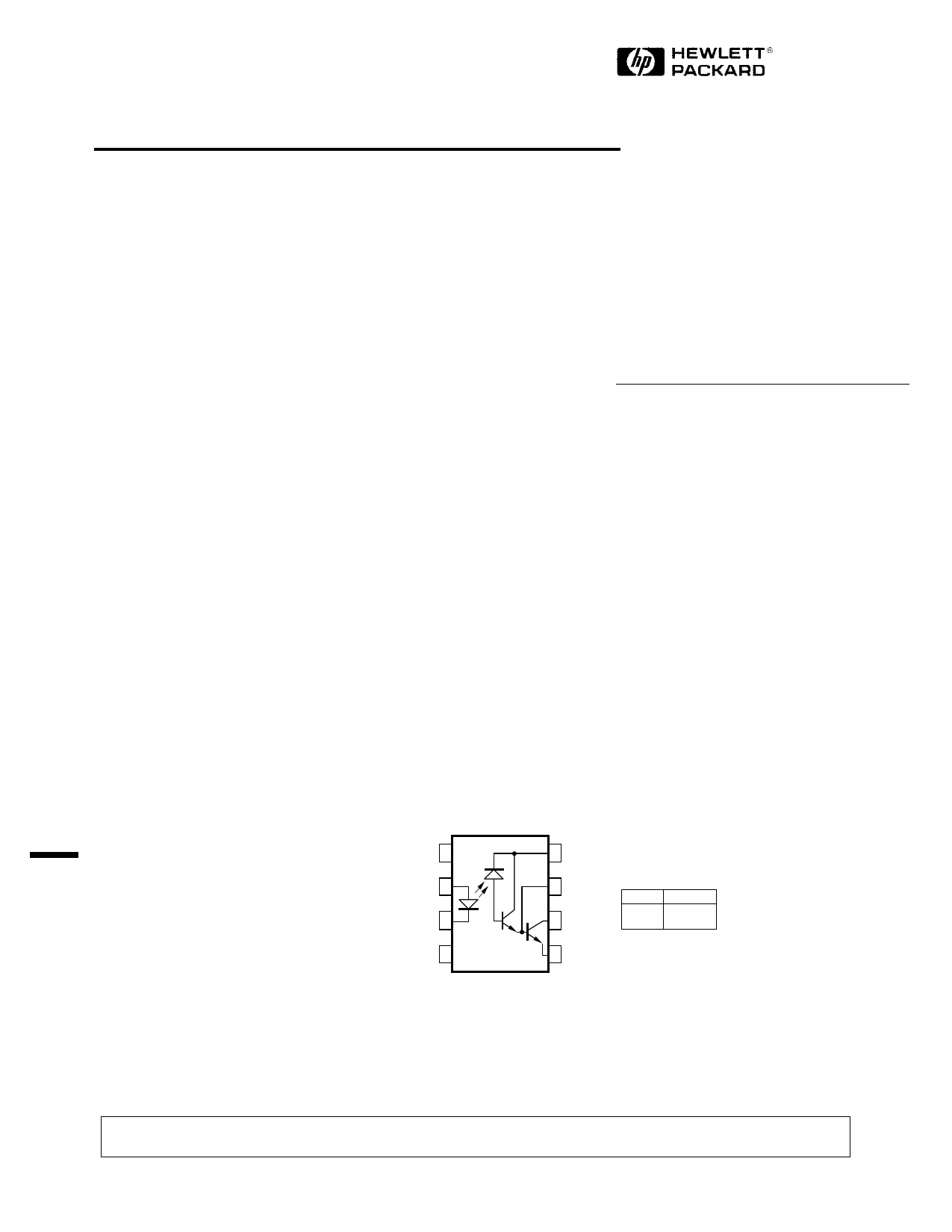
Functional Diagram
NC 1
ANODE 2
CATHODE 3
NC 4
8 VCC
7 VB
6 VO
5 GND
Description
These high gain series couplers
use a Light Emitting Diode and an
integrated high gain photodetec-
tor to provide extremely high
current transfer ratio between
input and output. Separate pins
for the photodiode and output
stage result in TTL compatible
saturation voltages and high
speed operation. Where desired
the VCC and VO terminals may be
tied together to achieve conven-
tional photodarlington operation.
A base access terminal allows a
gain bandwidth adjustment to be
made.
TRUTH TABLE
LED
ON
OFF
VO
LOW
HIGH
*5000 V rms/1 minute rating is for HCNW139/138 and Option 020 (6N139/138) products only.
A 0.1 µF bypass capacitor connected between pins 8 and 5 is recommended.
CAUTION: It is advised that normal static precautions be taken in handling and assembly of this component to
prevent damage and/or degradation which may be induced by ESD.
1 page 
5
Small Outline SO-8 Package (HCPL-0701/HCPL-0700)
8
3.937 ± 0.127
(0.155 ± 0.005)
PIN ONE 1
0.406 ± 0.076
(0.016 ± 0.003)
765
XXX
YWW
234
5.994 ± 0.203
(0.236 ± 0.008)
TYPE NUMBER
(LAST 3 DIGITS)
DATE CODE
1.270 BSG
(0.050)
* 5.080 ± 0.127
(0.200 ± 0.005)
7°
45°
X
0.432
(0.017)
3.175 ± 0.127
(0.125 ± 0.005)
1.524
(0.060)
0 ~ 7°
0.228 ± 0.025
(0.009 ± 0.001)
* TOTAL PACKAGE LENGTH (INCLUSIVE OF MOLD FLASH)
5.207 ± 0.254 (0.205 ± 0.010)
DIMENSIONS IN MILLIMETERS (INCHES).
LEAD COPLANARITY = 0.10 mm (0.004 INCHES) MAX.
0.203 ± 0.102
(0.008 ± 0.004)
0.305 MIN.
(0.012)
8-Pin Widebody DIP Package (HCNW139/HCNW138)
11.15 ± 0.15
(0.442 ± 0.006)
87
65
HP
HCNWXXXX
YYWW
1234
TYPE NUMBER
DATE CODE
1.55
(0.061)
MAX.
11.00
(0.433)
MAX.
9.00 ± 0.15
(0.354 ± 0.006)
10.16 (0.400)
TYP.
7° TYP.
(05.2.1001)MAX.
+ 0.076
0.254 - 0.0051
+ 0.003)
(0.010 - 0.002)
2.54 (0.100)
TYP.
1.78 ± 0.15
(0.070 ± 0.006)
3.10 (0.122)
3.90 (0.154)
0.51 (0.021) MIN.
0.40 (0.016)
0.56 (0.022)
DIMENSIONS IN MILLIMETERS (INCHES).
5 Page 
11
Switching Specifications (AC)
Over recommended operating conditions (TA = 0 to 70°C), VCC = 5 V, unless otherwise specified.
Parameter
Propagation Delay
Time to Logic Low at
Output
Propagation Delay
Time to Logic High
at Output
Common Mode
Transient Immunity
at Logic High Output
Common Mode
Transient Immunity
at Logic Low Output
Sym.
tPHL
Device
6N139
HCPL-0701
HCNW139
6N139
HCPL-0701
Min.
HCNW139
6N138
HCPL-0700
HCNW138
HCNW138
tPLH 6N139
HCPL-0701
HCNW139
HCNW139
6N139
HCPL-0701
HCNW139
HCNW139
6N138
HCPL-0700
HCNW138
6N138
HCPL-0700
HCNW139
|CMH|
1000
|CML|
1000
Typ.**
5
0.2
1.6
18
2
10
10000
10000
Max. Units
25* µs
30
1* µs
2
1.1
10* µs
15
11
60* µs
90
115
7* µs
10
1.1
35* µs
50
Test Conditions
TA = 25°C
IF = 0.5 mA,
Rl = 4.7 kΩ
TA = 25°C
IF = 12 mA,
Rl = 270 Ω
TA = 25°C
IF = 1.6 mA,
Rl = 2.2 kΩ
TA = 25°C
IF = 0.5 mA,
Rl = 4.7 kΩ
TA = 25°C
IF = 12 mA,
Rl = 270 Ω
TA = 25°C
IF = 1.6 mA,
Rl = 2.2 kΩ
70
V/µs IF = 0 mA,
TA = 25°C
Rl = 2.2 kΩ
V/µs
|VCM| = 10 Vp-p
IF = 1.6 mA,
TA = 25°C
Rl = 2.2 kΩ
|VCM| = 10 Vp-p
Fig. Note
5, 6, 2, 4
7, 9,
12
5, 6, 2, 4
7, 9,
12
13 5, 6
13 5, 6
*JEDEC Registered Data for 6N139 and 6N138.
**All typical values at TA = 25°C and VCC = 5 V, unless otherwise noted.
11 Page | ||
| Páginas | Total 16 Páginas | |
| PDF Descargar | [ Datasheet HCPL-0701.PDF ] | |
Hoja de datos destacado
| Número de pieza | Descripción | Fabricantes |
| HCPL-0700 | LOW INPUT CURRENT HIGH GAIN SPLIT DARLINGTON OPTOCOUPLERS | Fairchild Semiconductor |
| HCPL-0700 | Low Input Current/ High Gain Optocouplers | Agilent(Hewlett-Packard) |
| HCPL-0700 | LOW INPUT CURRENT HIGH GAIN SPLIT DARLINGTON OPTOCOUPLERS | Fairchild Semiconductor |
| HCPL-0700 | High Gain Optocouplers | Avago |
| Número de pieza | Descripción | Fabricantes |
| SLA6805M | High Voltage 3 phase Motor Driver IC. |
Sanken |
| SDC1742 | 12- and 14-Bit Hybrid Synchro / Resolver-to-Digital Converters. |
Analog Devices |
|
DataSheet.es es una pagina web que funciona como un repositorio de manuales o hoja de datos de muchos de los productos más populares, |
| DataSheet.es | 2020 | Privacy Policy | Contacto | Buscar |