|
|
|
PDF MT29F32G08GAAC6 Data sheet ( Hoja de datos )
| Número de pieza | MT29F32G08GAAC6 | |
| Descripción | NAND Flash Memory | |
| Fabricantes | Micron | |
| Logotipo | ||
Hay una vista previa y un enlace de descarga de MT29F32G08GAAC6 (archivo pdf) en la parte inferior de esta página. Total 30 Páginas | ||
|
No Preview Available !
Micron Confidential and Proprietary
Advance‡
8, 16, 32, 64Gb NAND Flash Memory
Features
NAND Flash Memory
MT29F8G08AAAWP, MT29F16G08DAAWP, MT29F32G08FAAWP,
MT29F8G08AAAC4, MT29F16G08EAAC4, MT29F32G08GAAC4,
MT29F8G08AAAC6, MT29F16G08EAAC6, MT29F32G08GAAC6,
MT29F64G08KAAC6
Features
• Open NAND Flash Interface (ONFI) 1.0 compliant
• Single-level cell (SLC) technology
• Organization
– Page size: x8: 4,314 bytes (4,096 + 218 bytes)
– Block size: 64 pages (256K + 13K bytes)
– Plane size: 2,048 blocks
– Device size: 8Gb: 4,096 blocks; 16Gb: 8,192 blocks;
32Gb: 16,384 blocks; 64Gb: 32,768 blocks
• READ performance
– Random READ: 25µs
– Sequential READ: 20ns
• WRITE performance
– PROGRAM PAGE: 250µs (TYP)
– BLOCK ERASE: 1.5ms (TYP)
• Endurance
– 100,000 PROGRAM/ERASE cycles (1-bit ECC1)
• Data retention: 10 years
• First block (block address 00h) guaranteed to be
valid when shipped from factory1
• Industry-standard basic NAND Flash command set
• Advanced command set
– PROGRAM PAGE CACHE MODE
– PAGE READ CACHE MODE
– One-time programmable (OTP) commands
– Two-plane commands
– Interleaved die operations
– READ UNIQUE ID (contact factory)
• Operation status byte provides a software method of
detecting:
– Operation completion
– Pass/fail condition
– Write-protect status
• Ready/busy# (R/B#) signal provides a hardware
method of detecting PROGRAM or ERASE cycle
completion
• WP# signal: entire device hardware write protect
• RESET required after power-up
• INTERNAL DATA MOVE operations supported
within the plane from which data is read
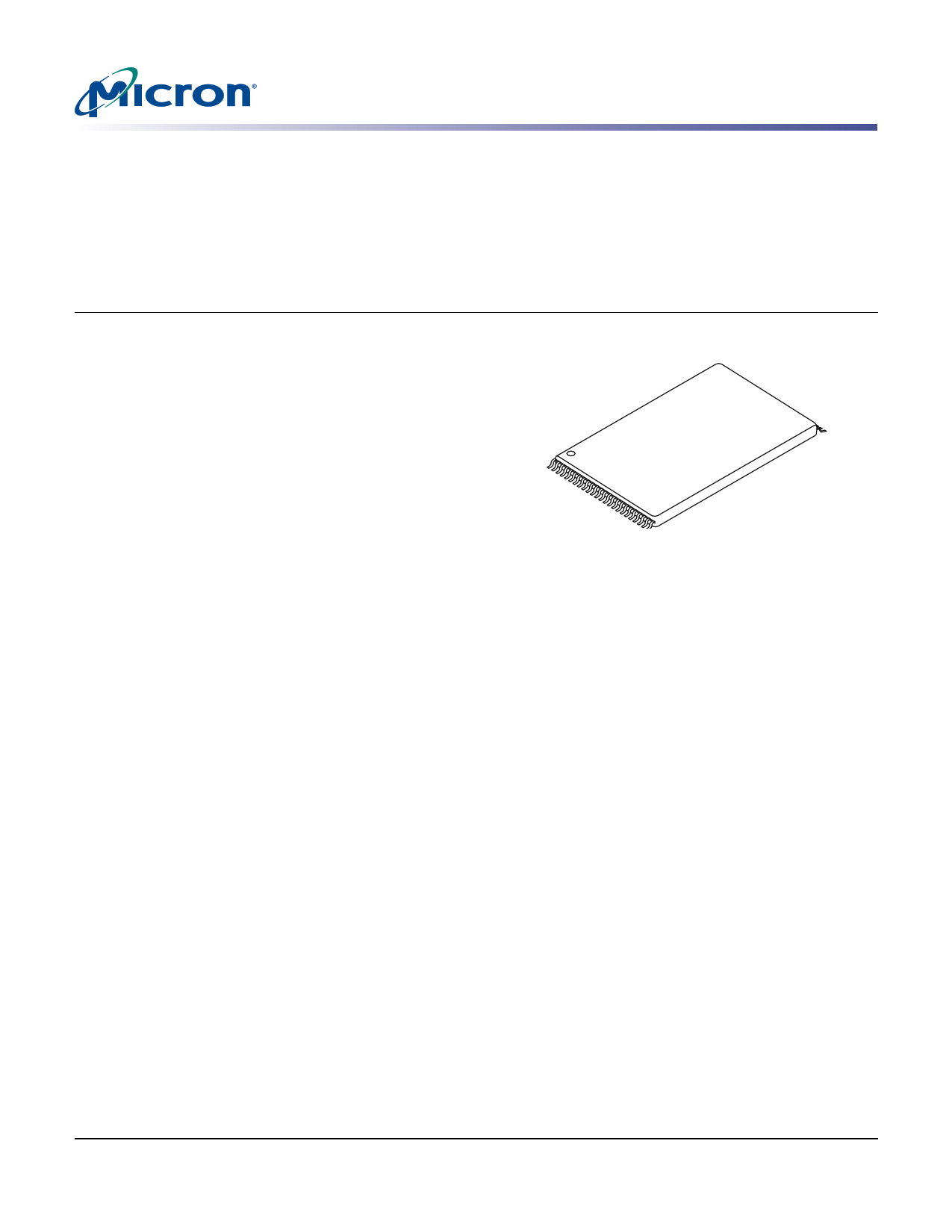
Figure 1: 48-Pin TSOP Type 1
Options
• Density2
– 8Gb, 16Gb, 32Gb, 64Gb
• Device width: x8
• Configuration:
# of die # of CE# # of R/B# I/O
TSOP/LGA 1
1
1 Common
TSOP 2
2
2 Common
TSOP 4
2
2 Common
LGA 2
2
2 Separate
LGA 4
2
2 Separate
LGA 8
4
4 Separate
• VCC: 2.7–3.6V
• Package:
– 48 TSOP type I (lead-free plating)
– 52-pad LGA
• Operating temperature:
– Commercial temperature (0°C to 70°C)
– Extended temperature (–40°C to +85°C)
Notes: 1. For details, see “Error Management” on
page 89.
2. For part numbering and markings, see
Figure 2 on page 2.
PDF: 09005aef82d68edc / Source: 09005aef82d68f88
8gb_nand_slc_m51a__1.fm -Rev. 1.9 5/08 EN
1 Micron Technology, Inc., reserves the right to change products or specifications without notice.
©2007 Micron Technology, Inc. All rights reserved.
‡Products and specifications discussed herein are for evaluation and reference purposes only and are subject to change by
Micron without notice. Products are only warranted by Micron to meet Micron’s production data sheet specifications.
1 page 
Micron Confidential and Proprietary
Advance
8, 16, 32, 64Gb NAND Flash Memory
List of Figures
List of Figures
Figure 1:
Figure 2:
Figure 3:
Figure 4:
Figure 5:
Figure 6:
Figure 7:
Figure 8:
Figure 9:
Figure 10:
Figure 11:
Figure 12:
Figure 13:
Figure 14:
Figure 15:
Figure 16:
Figure 17:
Figure 18:
Figure 19:
Figure 20:
Figure 21:
Figure 22:
Figure 23:
Figure 24:
Figure 25:
Figure 26:
Figure 27:
Figure 28:
Figure 29:
Figure 30:
Figure 31:
Figure 32:
Figure 33:
Figure 34:
Figure 35:
Figure 36:
Figure 37:
Figure 38:
Figure 39:
Figure 40:
Figure 41:
Figure 42:
Figure 43:
Figure 44:
Figure 45:
Figure 46:
Figure 47:
Figure 48:
Figure 49:
Figure 50:
Figure 51:
Figure 52:
Figure 53:
Figure 54:
Figure 55:
Figure 56:
48-Pin TSOP Type 1 . . . . . . . . . . . . . . . . . . . . . . . . . . . . . . . . . . . . . . . . . . . . . . . . . . . . . . . . . . . . . . . . . . . . . . . . . 1
Part Number Chart . . . . . . . . . . . . . . . . . . . . . . . . . . . . . . . . . . . . . . . . . . . . . . . . . . . . . . . . . . . . . . . . . . . . . . . . . 2
Pin Assignment (Top View) 48-Pin TSOP Type 1 . . . . . . . . . . . . . . . . . . . . . . . . . . . . . . . . . . . . . . . . . . . . . . . 9
Pad Assignment (Top View) 52-Pad VLGA . . . . . . . . . . . . . . . . . . . . . . . . . . . . . . . . . . . . . . . . . . . . . . . . . . . . 10
Pad Assignment (Top View) 52-Pad LLGA . . . . . . . . . . . . . . . . . . . . . . . . . . . . . . . . . . . . . . . . . . . . . . . . . . . . 11
NAND Flash Functional Block Diagram . . . . . . . . . . . . . . . . . . . . . . . . . . . . . . . . . . . . . . . . . . . . . . . . . . . . . . 13
Memory Map (x8) . . . . . . . . . . . . . . . . . . . . . . . . . . . . . . . . . . . . . . . . . . . . . . . . . . . . . . . . . . . . . . . . . . . . . . . . . 14
Array Organization for 8Gb and 16Gb x8 . . . . . . . . . . . . . . . . . . . . . . . . . . . . . . . . . . . . . . . . . . . . . . . . . . . . . 15
Array Organization for 32Gb and 64Gb x8 . . . . . . . . . . . . . . . . . . . . . . . . . . . . . . . . . . . . . . . . . . . . . . . . . . . . 16
READY/BUSY# Open Drain . . . . . . . . . . . . . . . . . . . . . . . . . . . . . . . . . . . . . . . . . . . . . . . . . . . . . . . . . . . . . . . . . 19
tFall and tRise . . . . . . . . . . . . . . . . . . . . . . . . . . . . . . . . . . . . . . . . . . . . . . . . . . . . . . . . . . . . . . . . . . . . . . . . . . . . . 20
Iol vs. Rp . . . . . . . . . . . . . . . . . . . . . . . . . . . . . . . . . . . . . . . . . . . . . . . . . . . . . . . . . . . . . . . . . . . . . . . . . . . . . . . . . . 20
TC vs. Rp . . . . . . . . . . . . . . . . . . . . . . . . . . . . . . . . . . . . . . . . . . . . . . . . . . . . . . . . . . . . . . . . . . . . . . . . . . . . . . . . . 20
PAGE READ Operation . . . . . . . . . . . . . . . . . . . . . . . . . . . . . . . . . . . . . . . . . . . . . . . . . . . . . . . . . . . . . . . . . . . . . 24
RANDOM DATA READ Operation . . . . . . . . . . . . . . . . . . . . . . . . . . . . . . . . . . . . . . . . . . . . . . . . . . . . . . . . . . . 25
READ ID Operation . . . . . . . . . . . . . . . . . . . . . . . . . . . . . . . . . . . . . . . . . . . . . . . . . . . . . . . . . . . . . . . . . . . . . . . . 25
READ PARAMETER PAGE (ECh) . . . . . . . . . . . . . . . . . . . . . . . . . . . . . . . . . . . . . . . . . . . . . . . . . . . . . . . . . . . . . 27
Status Register Operation for READ STATUS . . . . . . . . . . . . . . . . . . . . . . . . . . . . . . . . . . . . . . . . . . . . . . . . . 34
PAGE READ CACHE MODE Operation . . . . . . . . . . . . . . . . . . . . . . . . . . . . . . . . . . . . . . . . . . . . . . . . . . . . . . . 36
PROGRAM and READ STATUS Operation . . . . . . . . . . . . . . . . . . . . . . . . . . . . . . . . . . . . . . . . . . . . . . . . . . . . 37
RANDOM DATA INPUT . . . . . . . . . . . . . . . . . . . . . . . . . . . . . . . . . . . . . . . . . . . . . . . . . . . . . . . . . . . . . . . . . . . . 38
PROGRAM PAGE CACHE MODE Example . . . . . . . . . . . . . . . . . . . . . . . . . . . . . . . . . . . . . . . . . . . . . . . . . . . 39
INTERNAL DATA MOVE . . . . . . . . . . . . . . . . . . . . . . . . . . . . . . . . . . . . . . . . . . . . . . . . . . . . . . . . . . . . . . . . . . . 41
INTERNAL DATA MOVE with Optional Data Output and RANDOM DATA Input . . . . . . . . . . . . . . . . . 41
BLOCK ERASE Operation . . . . . . . . . . . . . . . . . . . . . . . . . . . . . . . . . . . . . . . . . . . . . . . . . . . . . . . . . . . . . . . . . . . 42
OTP DATA PROGRAM . . . . . . . . . . . . . . . . . . . . . . . . . . . . . . . . . . . . . . . . . . . . . . . . . . . . . . . . . . . . . . . . . . . . . 44
OTP PROGRAM with RANDOM DATA INPUT . . . . . . . . . . . . . . . . . . . . . . . . . . . . . . . . . . . . . . . . . . . . . . . . 45
OTP DATA PROTECT . . . . . . . . . . . . . . . . . . . . . . . . . . . . . . . . . . . . . . . . . . . . . . . . . . . . . . . . . . . . . . . . . . . . . . 46
OTP DATA READ Operation . . . . . . . . . . . . . . . . . . . . . . . . . . . . . . . . . . . . . . . . . . . . . . . . . . . . . . . . . . . . . . . . 47
OTP DATA READ with RANDOM DATA READ . . . . . . . . . . . . . . . . . . . . . . . . . . . . . . . . . . . . . . . . . . . . . . . . 48
GET FEATURES Operation . . . . . . . . . . . . . . . . . . . . . . . . . . . . . . . . . . . . . . . . . . . . . . . . . . . . . . . . . . . . . . . . . 51
SET FEATURES Operation . . . . . . . . . . . . . . . . . . . . . . . . . . . . . . . . . . . . . . . . . . . . . . . . . . . . . . . . . . . . . . . . . . 52
TWO-PLANE PAGE READ . . . . . . . . . . . . . . . . . . . . . . . . . . . . . . . . . . . . . . . . . . . . . . . . . . . . . . . . . . . . . . . . . . 55
TWO-PLANE PAGE READ with RANDOM DATA READ . . . . . . . . . . . . . . . . . . . . . . . . . . . . . . . . . . . . . . . . 56
TWO-PLANE PROGRAM PAGE . . . . . . . . . . . . . . . . . . . . . . . . . . . . . . . . . . . . . . . . . . . . . . . . . . . . . . . . . . . . . . 57
TWO-PLANE PROGRAM PAGE with RANDOM DATA INPUT . . . . . . . . . . . . . . . . . . . . . . . . . . . . . . . . . . . 58
TWO-PLANE PROGRAM PAGE CACHE MODE . . . . . . . . . . . . . . . . . . . . . . . . . . . . . . . . . . . . . . . . . . . . . . . 60
TWO-PLANE INTERNAL DATA MOVE . . . . . . . . . . . . . . . . . . . . . . . . . . . . . . . . . . . . . . . . . . . . . . . . . . . . . . . 62
TWO-PLANE INTERNAL DATA MOVE with TWO-PLANE RANDOM DATA READ . . . . . . . . . . . . . . . . 63
TWO-PLANE INTERNAL DATA MOVE with RANDOM DATA INPUT . . . . . . . . . . . . . . . . . . . . . . . . . . . . 64
TWO-PLANE BLOCK ERASE Operation . . . . . . . . . . . . . . . . . . . . . . . . . . . . . . . . . . . . . . . . . . . . . . . . . . . . . . 65
TWO-PLANE/MULTIPLE-DIE READ STATUS Cycle . . . . . . . . . . . . . . . . . . . . . . . . . . . . . . . . . . . . . . . . . . . 66
Interleaved PAGE READ with Status Register Monitoring . . . . . . . . . . . . . . . . . . . . . . . . . . . . . . . . . . . . . . 68
Interleaved TWO-PLANE PAGE READ with Status Register Monitoring . . . . . . . . . . . . . . . . . . . . . . . . . . 70
Interleaved PROGRAM PAGE with Status Register Monitoring . . . . . . . . . . . . . . . . . . . . . . . . . . . . . . . . . . 71
Interleaved PROGRAM PAGE CACHE MODE with Status Register Monitoring . . . . . . . . . . . . . . . . . . . 71
Interleaved TWO-PLANE PROGRAM PAGE with Status Register Monitoring . . . . . . . . . . . . . . . . . . . . . 73
Interleaved TWO-PLANE PROGRAM PAGE CACHE MODE with Status Register Monitoring . . . . . . . 75
Interleaved READ for INTERNAL DATA MOVE with Status Register Monitoring . . . . . . . . . . . . . . . . . . 77
Interleaved TWO-PLANE READ for INTERNAL DATA MOVE with Status Register Monitoring . . . . . 79
Interleaved PROGRAM for INTERNAL DATA MOVE with Status Register Monitoring . . . . . . . . . . . . . 80
Interleaved TWO-PLANE PROGRAM for INTERNAL DATA MOVE with Status Register Monitoring . 81
Interleaved BLOCK ERASE with Status Register Monitoring . . . . . . . . . . . . . . . . . . . . . . . . . . . . . . . . . . . . 82
Interleaved TWO-PLANE BLOCK ERASE with Status Register Monitoring . . . . . . . . . . . . . . . . . . . . . . . 83
RESET Operation . . . . . . . . . . . . . . . . . . . . . . . . . . . . . . . . . . . . . . . . . . . . . . . . . . . . . . . . . . . . . . . . . . . . . . . . . . 85
ERASE Enable . . . . . . . . . . . . . . . . . . . . . . . . . . . . . . . . . . . . . . . . . . . . . . . . . . . . . . . . . . . . . . . . . . . . . . . . . . . . . 86
PDF: 09005aef82d68edc / Source: 09005aef82d68f88
8gb_nand_slc_m51aLOF.fm -Rev. 1.9 5/08 EN
5 Micron Technology, Inc., reserves the right to change products or specifications without notice.
©2007 Micron Technology, Inc. All rights reserved.
5 Page 
Micron Confidential and Proprietary
Advance
8, 16, 32, 64Gb NAND Flash Memory
General Description
Figure 5: Pad Assignment (Top View) 52-Pad LLGA
0 12 3 4 567
8
NC
OA CE4#2
A CE3#2
CLE
B VSS
OB NC
C ALE
CLE21
D ALE21
OC DNU
E WE2#1
WE#
F WP#
G I/O0-21
I/O0
H I/O1
J I/O1-21
I/O2
OD DNU/
VSS
K
I/O3
L I/O2-21
OE NC
VSS
M VSS
N
DNU/
VCC
OF NC
I/O3-21
CE# R/B3#2
VCC
CE2#1
RE#
RE2#1
R/B# R/B2#1
VSS
WP2#1
I/O7-21
I/O7
I/O6 I/O6-21
I/O5
I/O4 I/O5-21
VCC
I/O4-21
DNU/
VCC
R/B4#22
NC
DNU
DNU
DNU/
VSS
NC
Top View, Pads Down
Notes: 1. These signals are available only on the 16Gb, 32Gb, and 64Gb devices. These pads are NC
for other configurations.
2. These signals are available only on the 64Gb device. These pads are NC for other configu-
rations.
PDF: 09005aef82d68edc / Source: 09005aef82d68f88
8gb_nand_slc_m51a__2.fm -Rev. 1.9 5/08 EN
11
Micron Technology, Inc., reserves the right to change products or specifications without notice.
©2007 Micron Technology, Inc. All rights reserved.
11 Page | ||
| Páginas | Total 30 Páginas | |
| PDF Descargar | [ Datasheet MT29F32G08GAAC6.PDF ] | |
Hoja de datos destacado
| Número de pieza | Descripción | Fabricantes |
| MT29F32G08GAAC4 | NAND Flash Memory | Micron |
| MT29F32G08GAAC6 | NAND Flash Memory | Micron |
| Número de pieza | Descripción | Fabricantes |
| SLA6805M | High Voltage 3 phase Motor Driver IC. |
Sanken |
| SDC1742 | 12- and 14-Bit Hybrid Synchro / Resolver-to-Digital Converters. |
Analog Devices |
|
DataSheet.es es una pagina web que funciona como un repositorio de manuales o hoja de datos de muchos de los productos más populares, |
| DataSheet.es | 2020 | Privacy Policy | Contacto | Buscar |