|
|
PDF HD64645F Data sheet ( Hoja de datos )
| Número de pieza | HD64645F | |
| Descripción | LCTC (LCD Timing Controller) | |
| Fabricantes | Hitachi Semiconductor | |
| Logotipo | ||
Hay una vista previa y un enlace de descarga de HD64645F (archivo pdf) en la parte inferior de esta página. Total 30 Páginas | ||
|
No Preview Available !
HD64645/HD64646
LCTC (LCD Timing Controller)
ADE-207-276(Z)
'99.9
Rev. 0.0
Description
The HD64645/HD64646 LCTC is a control LSI for large size dot matrix liquid crystal displays. The LCTC
is software compatible with the HD6845 CRTC, since its programming method of internal registers and
memory addresses is based on the CRTC. A display system can be easily converted from a CRT to an
LCD.
The HD64646 LCTC is a modified version of the HD64645 LCTC with different LCD interface timing.
The LCTC offers a variety of functions and performance features such as vertical and horizontal scrolling,
and various types of character attribute functions such as reverse video, blinking, nondisplay (white or
black), and an OR function for simple superimposition of character and graphic displays. The LCTC also
provides DRAM refresh address output.
A compact LCD system with a large screen can be configured by connecting the LCTC with the
HD66110ST (column driver) and the HD66113T (common driver) by utilizing 4-bit × 2 data outputs.
Power dissipation has been lowered by adopting the CMOS process.
Features
• Software compatible with the HD6845 CRTC
• Programmable screen size
Up to 1024 dots (height)
Up to 4096 dots (width)
• High-speed data transfer
Up to 20 Mbits/s in character mode
Up to 40 Mbits/s in graphic mode
• Selectable single or dual screen configuration
• Programmable multiplexing duty ratio: static to 1/512 duty cycle
• Programmable character font
1-32 dots (height)
8 dots (width)
1
1 page 
HD64645/64646
Pin Functions
Power Supply (VCC1, VCC2, GND)
Power Supply Pin (+5 V): Connect VCC1 and VCC2 with +5V power supply circuit.
Ground Pin (0 V): Connect GND1 and GND2 with 0V.
LCD Interface
LCD Up Panel Data (LU0–LU3), LCD Down Panel Data (LD0–LD3): LU0–LU3 and LD0–LD3 output
LCD data as shown in Table 1.
Clock One (CL1): CL1 supplies timing clocks for display data latch.
Clock Two (CL2): CL2 supplies timing clock for display data shift.
First Line Marker (FLM): FLM supplies first line marker.
M (M): M converts liquid crystal drive output to AC.
Memory Interface
Memory Address (MA0–MA15): MA0–MA15 supply the display memory address.
Raster Address (RA0–RA4): RA0–RA4 supply the raster address.
Memory Data (MD0–MD7): MD0–MD7 receive the character dot data or bit-mapped data.
Memory Data (MD8–MD15): MD8–MD15 receive attribute code data or bit-mapped data.
MPU Interface
Data Bus (DB0–DB7): DB0–DB7 send/receive data as a three-state I/O common bus.
Chip Select (CS): CS selects a chip. Low level enables MPU read/write of the LCTC internal registers.
Write (WR): WR receives MPU write strobe.
Read (RD): RD receives MPU read strobe.
Register Select (RS): RS selects registers. (Refer to Table 4.)
Reset (RES): RES performs external reset of the LCTC. Low level of RES stops and zero-clears the LCTC
internal counter. No register contents are affected.
5
5 Page 
HD64645/64646
Internal Block Diagram
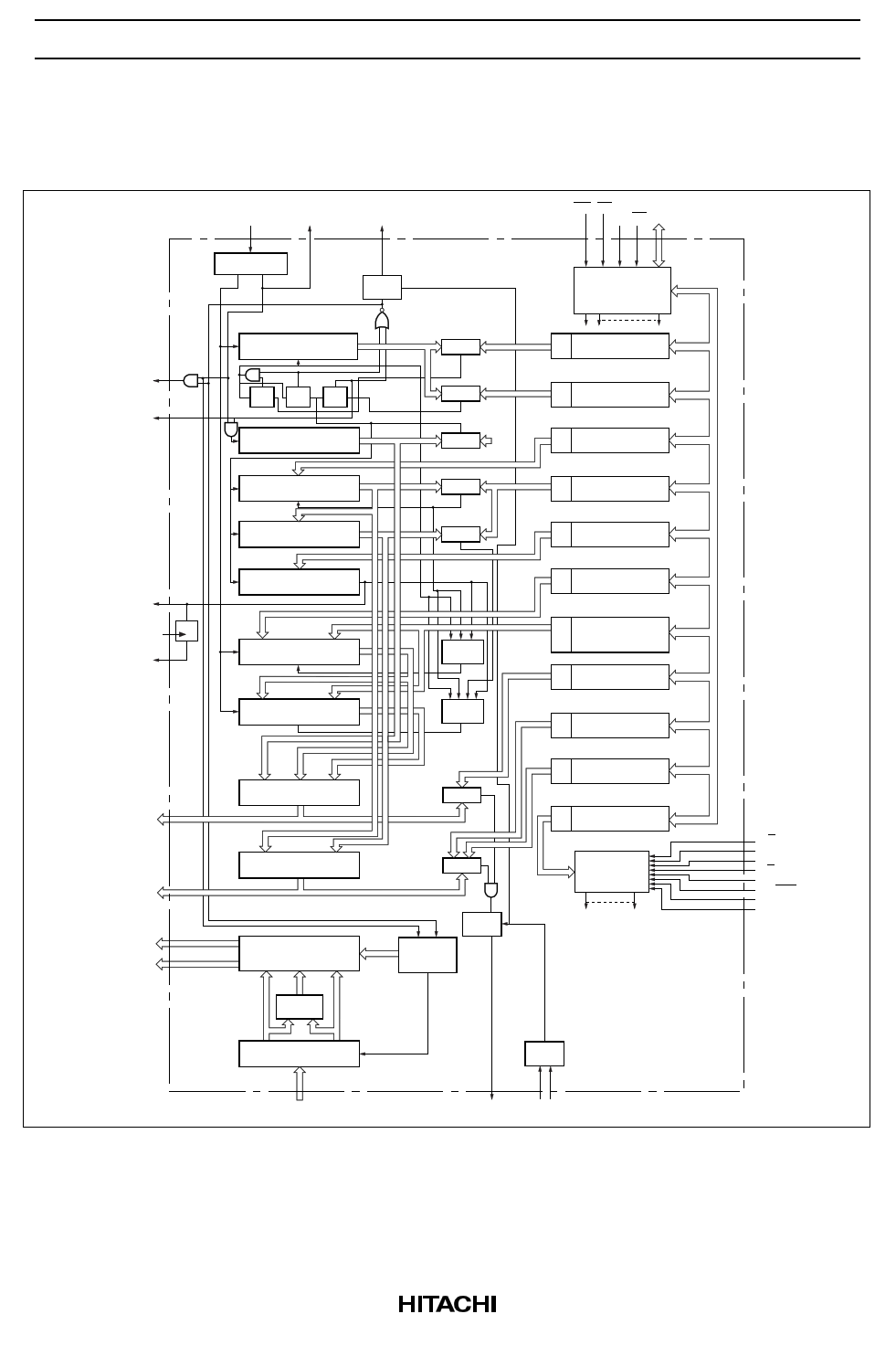
Figure 3 is a block diagram of the LCTC.
CL2
CL1
FLM
Counter 1/2
M
MA0–MA15
RA0–RA4
LU0–LU3
LD0–LD3
DCLK
MCLK
DISPTMG
Dot counter
CPMA MCLK
Skew
control
CLK
Character counter
(8 bits)
RQS RQS RQS
CLK
Refresh address
counter (8 bits)
CLK
Upper panel raster
counter (5 bits)
MR
CLK
Down panel raster
counter (5 bits)
CLK
Multiplexing duty
ratio counter (9 bits)
CMP
CMP
CMP 16
CMP
CMP
CLK
Upper panel address
counter (16 bits)
CLK
Down panel address
counter (16 bits)
Counter
control
Counter
control
MPX
CMP
WR RD
RS CS DB0–DB7
Address register
&
R/W control
R0
Horizontal total
register (W)
R1
Horizontal displayed
register (W)
R21
Display start raster
register (W)
R9
Maximum raster
address register (W)
R19 Multiplexing duty
R20 ratio register (W)
R12 Start address
R13 register (R/W)
Horizontal virtual
R18 screen width
register (R/W)
R14 Cursor address
R15 register (R/W)
R10
Cursor start raster
register (W)
R11
Cursor end raster
register (W)
R22 Mode register (W)
MPX
8-bit/4-bit counter
Attribute
control
Input register
CMP
Data
conversion
control
Skew
control
Mode control
circuit
Skew
circuit
MD0–MD15
CUDISP SK0 SK1
Figure 3 LCTC Block Diagram
G/C
AT
LS
D/S
WIDE
ON/OFF
MODE
BLE
11
11 Page | ||
| Páginas | Total 30 Páginas | |
| PDF Descargar | [ Datasheet HD64645F.PDF ] | |
Hoja de datos destacado
| Número de pieza | Descripción | Fabricantes |
| HD64645 | LCTC (LCD Timing Controller) | Hitachi Semiconductor |
| HD64645F | LCTC (LCD Timing Controller) | Hitachi Semiconductor |
| Número de pieza | Descripción | Fabricantes |
| SLA6805M | High Voltage 3 phase Motor Driver IC. |
Sanken |
| SDC1742 | 12- and 14-Bit Hybrid Synchro / Resolver-to-Digital Converters. |
Analog Devices |
|
DataSheet.es es una pagina web que funciona como un repositorio de manuales o hoja de datos de muchos de los productos más populares, |
| DataSheet.es | 2020 | Privacy Policy | Contacto | Buscar |
