|
|
PDF IXDN514 Data sheet ( Hoja de datos )
| Número de pieza | IXDN514 | |
| Descripción | 14 Ampere Low-Side Ultrafast MOSFET Drivers | |
| Fabricantes | IXYS | |
| Logotipo |  |
|
Hay una vista previa y un enlace de descarga de IXDN514 (archivo pdf) en la parte inferior de esta página. Total 12 Páginas | ||
|
No Preview Available !
Preliminary Technical Information
IXDI514 / IXDN514
14 Ampere Low-Side Ultrafast MOSFET Drivers
Features
• Built using the advantages and compatibility
of CMOS and IXYS HDMOSTM processes
• Latch-Up Protected over entire Operating Range
• High Peak Output Current: 14A Peak
• Wide Operating Range: 4.5V to 30V
• -55°C to +125°C Extended Operating
Temperature
• High Capacitive Load
Drive Capability: 15nF in <30ns
• Matched Rise And Fall Times
• Low Propagation Delay Time
• Low Output Impedance
• Low Supply Current
• Two Drivers in Single Chip
Applications
• Driving MOSFETs and IGBTs
• Motor Controls
• Line Drivers
• Pulse Generators
• Local Power ON/OFF Switch
• Switch Mode Power Supplies (SMPS)
• DC to DC Converters
• Pulse Transformer Driver
• Class D Switching Amplifiers
• Power Charge Pumps
General Description
The IXDI514 and IXDN514 are high speed high current gate
drivers specifically designed to drive the largest IXYS
MOSFETs & IGBTs to their minimum switching time and
maximum parctical frequency limits. The IXDI514 and
IXDN514 can source and sink 14 Amps of Peak Current
while producing voltage rise and fall times of less than
30ns. The inputs of the Drivers are compatible with TTL or
CMOS and are virtually immune to latch up over the entire
operating range! Patented* design innovations eliminate
cross conduction and current "shoot-through". Improved
speed and drive capabilities are further enhanced by very
quick & matched rise and fall times.
The IXDI514 is configured as a Inverting Gate Driver, and the
IXDN514 is configured as a Non-Inverting Gate Driver.
The IXDI514 and IXDN514 are each available in the 8-Pin P-
DIP (PI) package, the 8-Pin SOIC (SIA) package, and the
6-Lead DFN (D1) package, (which occupies less than 65%
of the board area of the 8-Pin SOIC).
*United States Patent 6,917,227
Ordering Information
Part Number
IXDI514PI
IXDI514SIA
IXDI514SIAT/R
IXDI514D1
IXDI514D1T/R
IXDN514PI
IXDN514SIA
IXDN514SIAT/R
IXDN514D1
IXDN514D1T/R
Description
14A Low Side Gate Driver I.C.
14A Low Side Gate Driver I.C.
14A Low Side Gate Driver I.C.
14A Low Side Gate Driver I.C.
14A Low Side Gate Driver I.C.
14A Low Side Gate Driver I.C.
14A Low Side Gate Driver I.C.
14A Low Side Gate Driver I.C.
14A Low Side Gate Driver I.C.
14A Low Side Gate Driver I.C.
Package
Type
8-Pin PDIP
8-Pin SOIC
8-Pin SOIC
6-Lead DFN
6-Lead DFN
8-Pin PDIP
8-Pin SOIC
8-Pin SOIC
6-Lead DFN
6-Lead DFN
Packing Style
Tube
Tube
13” Tape and Reel
2” x 2”Waffle Pack
13” Tape and Reel
Tube
Tube
13” Tape and Reel
2” x 2” Waffle Pack
13” Tape and Reel
Pack
Qty
50
94
2500
56
2500
50
94
2500
56
2500
Configuration
Inverting
Non-Inverting
NOTE: All parts are lead-free and RoHS Compliant
Copyright © 2006 IXYS CORPORATION All rights reserved
First Release
DS99672(01/07)
http://www.Datasheet4U.com
1 page 
IXDI514 / IXDN514
* The following notes are meant to define the conditions for thθeJ-A, θJ-C and θJ-S values:
1) TheθJ-A (typ) is defined as junction to ambient. ThθeJ-A of the standard single die 8-Lead PDIP and 8-Lead SOIC are dominated by the
resistance of the package, and the IXD_5XX are typical. The values for these packages are natural convection values withcavlebrtoi ards
and the values would be lower with natural convection. For the 6-Lead DFN package,θtJh-Aevalue supposes the DFN package is soldered
on a PCB. TheθJ-A (typ) is 200°C/W with no special provisions on the PCB, but because the center pad provides a low thermal resistance
to the die, it is easy to reduce theθJ-A by adding connected copper pads or traces on the PCB. These can reduce theθJ-A (typ) to 125°C/W
easily, and potentially even lower. TheθJ-Afor DFN on PCB without heatsink or thermal management will vary significantly with size,
construction, layout, materials, etc. This typical range tells the user what he is likely to get if he does no thermal manageenmt.
2) θJ-C (max) is defined as juction to case, where case is the large pad on the back of the DFN package. θTJh-Cevalues are generally not
published for the PDIP and SOIC packages. ThθeJ-Cfor the DFN packages are important to show the low thermal resistance from junction to
the die attach pad on the back of the DFN, -- and a guardband has been added to be safe.
3) TheθJ-S (typ) is defined as junction to heatsink, where the DFN package is soldered to a thermal substrate that is mounted on a nhke.atsi
The value must be typical because there are a variety of thermal substrates. This value was calculated based on easily alveaIiMlabS in the
U.S. or Europe, and not a premium Japanese IMS. A 4 mil dialectric with a thermal conductivity of 2.2W/mC was assumed.sTulhtewraes
given as typical, and indicates what a user would expect on a typical IMS substrate, and shows the potential low thermal raensciset for the
DFN package.
Pin Description
SYMBOL FUNC
TION
VCC Sup
ply Voltage
IN Input
OUT
Output
GND G
round
DESCRIPTION
Positive p ower-supply voltage input. T his pi n provides po wer to t he
entire chip. The range for this voltage is from 4.5V to 30V.
Input signal-TTL or CMOS compatible.
Driver O utput. For a pplication p urposes, t his p in is c onnected,
through a resistor, to Gate of a MOSFET/IGBT.
The system ground pin. Internally connected to all circuitry, this pin
provides ground reference for the entire chip. This pin should be
connected to a low noise analog ground plane for optimum
performance.
CAUTION: Follow proper ESD procedures when handling and assembling this component.
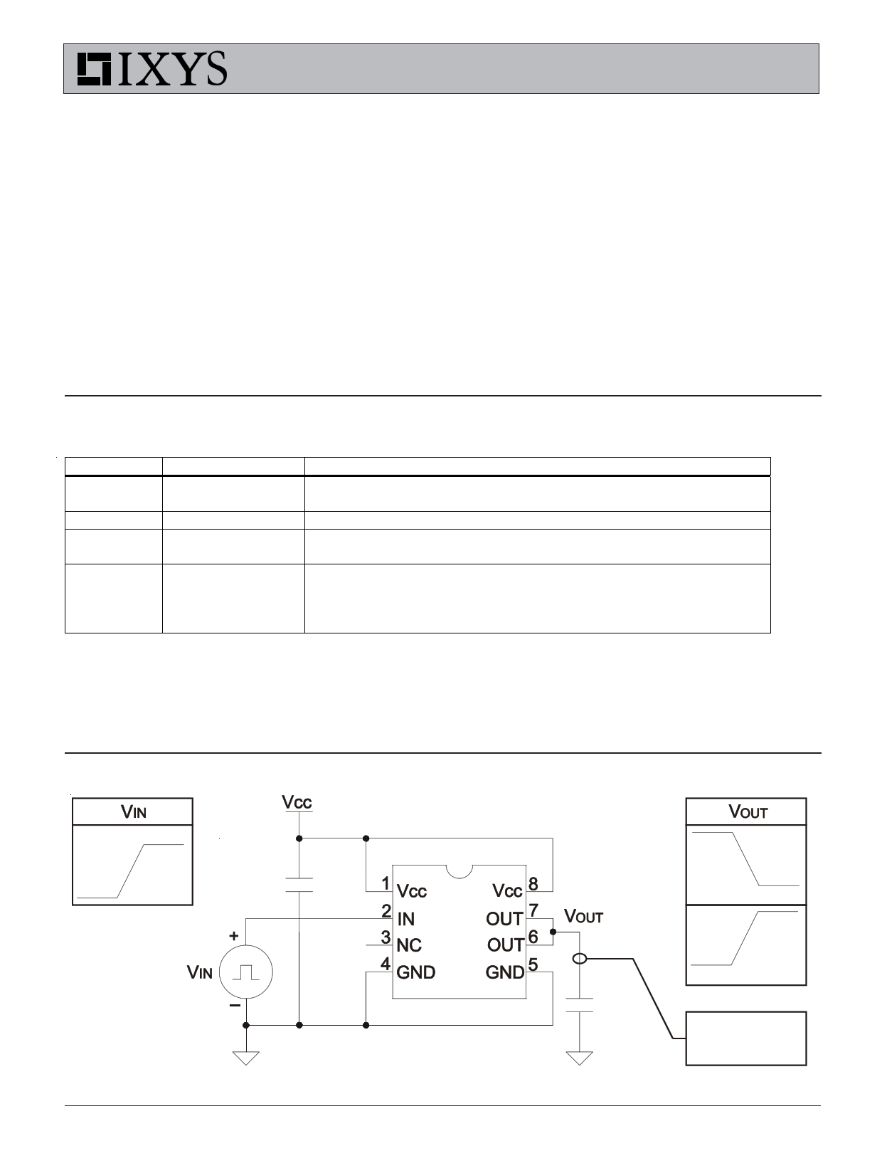
Figure 3 - Characteristics Test Diagram
5.0V
0V
10uF
25V
21550n0 pFf
Vcc
0V
IXDI4514
Vcc
0V
IXIXDDNN451144
Agilent 1147A
Current Probe
5
5 Page 
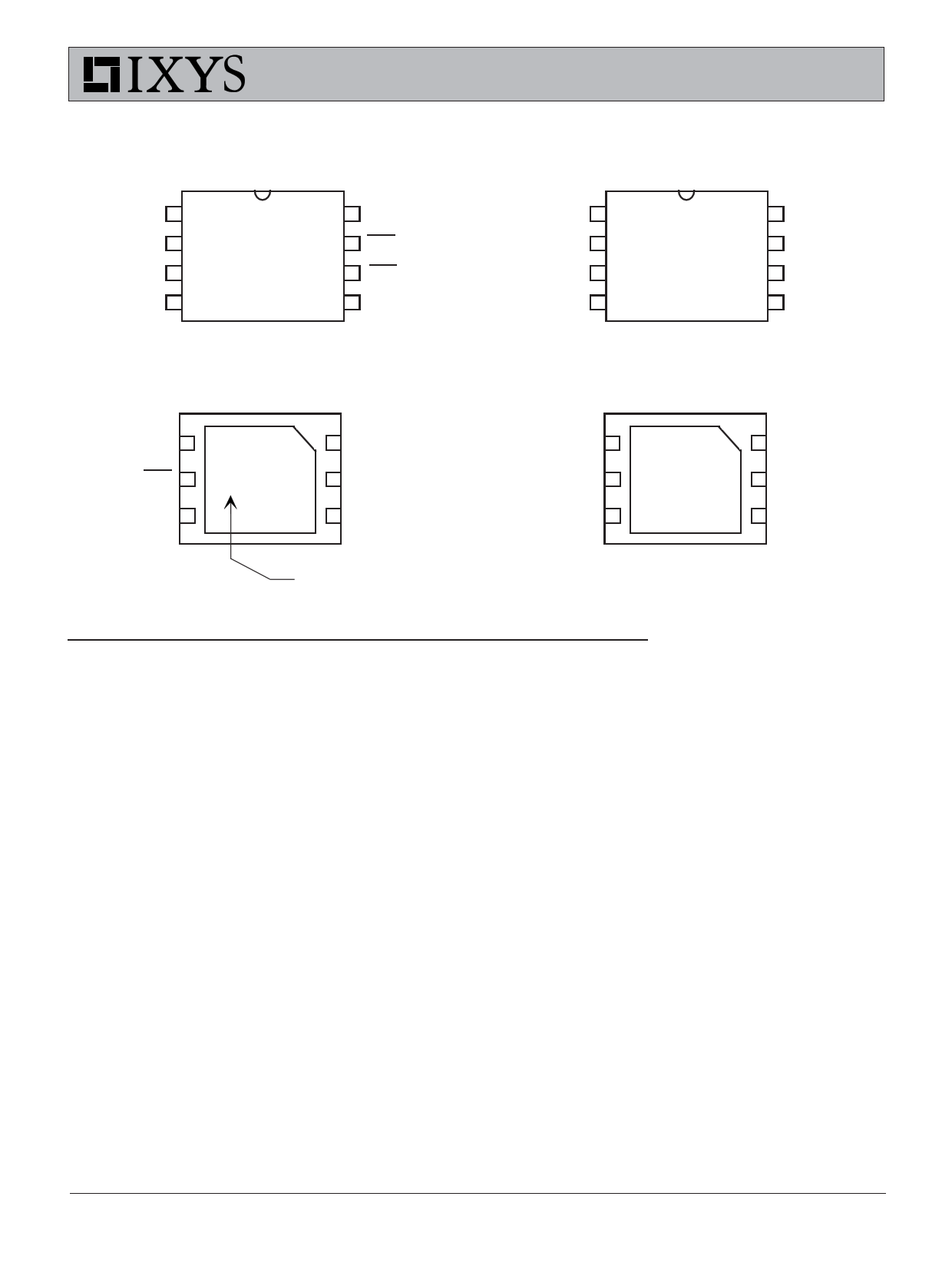
PIN CONFIGURATIONS
8 PIN DIP (PI)
8 PIN SOIC (SIA)
VCC 1
IN 2
NC 3
GND 4
I 8 VCC
X
D 7 OUT
I
5 6 OUT
1
4 5 GND
IXDI514 / IXDN514
VCC 1
IN 2
NC 3
GND 4
8 PIN DIP (PI)
8 PIN SOIC (SIA)
I 8 VCC
X
D 7 OUT
N
5 6 OUT
1
4 5 GND
6 LEAD DFN (D1)
(Bottom View)
VCC 6
I
X
1 IN
D
OUT 5 I 2 N /C
5
GND 4 1 3 GND
4
6 LEAD DFN (D1)
(Bottom View)
VCC 6
I
X
1 IN
D
OUT 5 N 2 N /C
5
GND 4 1 3 GND
4
NOTE: Solder tabs on bottoms of DFN packages are grounded
Supply Bypassing, Grounding Practices And Output Lead inductance
When designing a circuit to drive a high speed MOSFET
GROUNDING
utilizing the IXD_514, it is very important to observe certain
In order for the design to turn the load off properly, the IXD_514
design criteria in order to optimize performance of the driver.
must be able to drain this 5A of current into an adequate
Particular attention needs to be paid to Supply Bypassing , grounding system. There are three paths for returning current
Grounding, and minimizing the Output Lead Inductance.
that need to be considered: Path #1 is between the IXD_514
and its load. Path #2 is between the IXD_514 and its power
Say, for example, we are using the IXD_514 to charge a 5000pF supply. Path #3 is between the IXD_514 and whatever logic is
capacitive load from 0 to 25 volts in 25ns .
driving it. All three of these paths should be as low in resistance
and inductance as possible, and thus as short as practical. In
Using the formula: I= ∆V C / ∆t, where ∆V=25V C=5000pF & addition, every effort should be made to keep these three
∆t=25ns, we can determine that to charge 5000pF to 25 volts
ground paths distinctly separate. Otherwise, the returning
in 25ns will take a constant current of 5A. (In reality, the charging ground current from the load may develop a voltage that would
current won’t be constant, and will peak somewhere around
have a detrimental effect on the logic line driving the IXD_514.
8A).
SUPPLY BYPASSING
In order for our design to turn the load on properly, the IXD_514
must be able to draw this 5A of current from the power supply
in the 25ns. This means that there must be very low impedance
between the driver and the power supply. The most common
method of achieving this low impedance is to bypass the power
supply at the driver with a capacitance value that is an order of
magnitude larger than the load capacitance. Usually, this
would be achieved by placing two different types of bypassing
capacitors, with complementary impedance curves, very close
to the driver itself. (These capacitors should be carefully
selected and should have low inductance, low resistance and
high-pulse current-service ratings). Lead lengths may radiate
at high frequency due to inductance, so care should be taken
to keep the lengths of the leads between these bypass
capacitors and the IXD_514 to an absolute minimum.
OUTPUT LEAD INDUCTANCE
Of equal importance to Supply Bypassing and Grounding are
issues related to the Output Lead Inductance. Every effort
should be made to keep the leads between the driver and its
load as short and wide as possible. If the driver must be placed
farther than 2” (5mm) from the load, then the output leads
should be treated as transmission lines. In this case, a twisted-
pair should be considered, and the return line of each twisted
pair should be placed as close as possible to the ground pin
of the driver, and connected directly to the ground terminal of the
load.
11
11 Page | ||
| Páginas | Total 12 Páginas | |
| PDF Descargar | [ Datasheet IXDN514.PDF ] | |
Hoja de datos destacado
| Número de pieza | Descripción | Fabricantes |
| IXDN514 | 14 Ampere Low-Side Ultrafast MOSFET Drivers | IXYS |
| Número de pieza | Descripción | Fabricantes |
| SLA6805M | High Voltage 3 phase Motor Driver IC. |
Sanken |
| SDC1742 | 12- and 14-Bit Hybrid Synchro / Resolver-to-Digital Converters. |
Analog Devices |
|
DataSheet.es es una pagina web que funciona como un repositorio de manuales o hoja de datos de muchos de los productos más populares, |
| DataSheet.es | 2020 | Privacy Policy | Contacto | Buscar |
