|
|
PDF AK8131C Data sheet ( Hoja de datos )
| Número de pieza | AK8131C | |
| Descripción | Multi Clock Generator | |
| Fabricantes | AKM | |
| Logotipo |  |
|
Hay una vista previa y un enlace de descarga de AK8131C (archivo pdf) en la parte inferior de esta página. Total 8 Páginas | ||
|
No Preview Available !
ASAHI KASEI EMD CORPORATION
Low Power
Multiclock Generator with VCXO
AK8131C
Features
27MHz Crystal Input
Clock out Frequencies:
REFOUT: 27.000MHz
CLK1:
33.000MHz
CLK2:
33.000MHz
CLK3:
27.000MHz
CLK4:
27.000MHz
Built-in VCXO
- Pull Range: ±100ppm (Min.)
Low Jitter Performance
- Period Jitter :
120 psec (Typ.) at CLK1/CLK2
- Long Term Jitter :
160 psec (Typ.) at REFOUT/CLK3/4
Low Current Consumption:
10.0mA (Typ.) at 3.3V
Supply Voltage:
3.0 – 3.6V
Operating Temperature Range:
-20 to +85℃
Package:
16-pin SSOP (Lead free)
Description
The AK8131C is a member of AKEMD’s low power
multi clock generator family designed for a feature
rich DTV or STB, requiring a range of system
clocks with high performance. The on-chip
VCXO accepts a voltage control input to allow the
output clocks to vary by ±100 ppm for
synchronizing to the external clock system. Both
circuitries of VCXO and PLL in AK8131C are
derived from AKEMD’s long-term-experienced
clock device technology, and enable clock output
to perform low jitter and to operate with very low
current consumption. The AK8131C is available
in a 16-pin SSOP package.
Applications
Digital TV Sets
Personal Video Recorders
Set-Top-Boxes
Multi Media Receivers
Block Diagram
VDD
X1
Voltage
Controlled
Crystal
X2 Oscillator
VIN
S0
S1
S2
PLL1
PLL1
Divide
Logic
and
Output
Control
CLK1
CLK2
CLK3
CLK4
REFOUT
GND
AK8131C Multi Clock Generator
MS0944-E-00
-1-
Mar-08
http://www.Datasheet4U.com
1 page 
The brand name
of AKEMD’s IC’s
AK8131C
Output clock frequency selection
The AK8131C generates a range of low-jitter and hi-accuracy clock frequency with a built-in PLL and
provides to up to four assigned outputs. A frequency selection at assigned output pin is configured by
pin-setting of S0 (Pin2), S1 (Pin3), and S2 (Pin14).
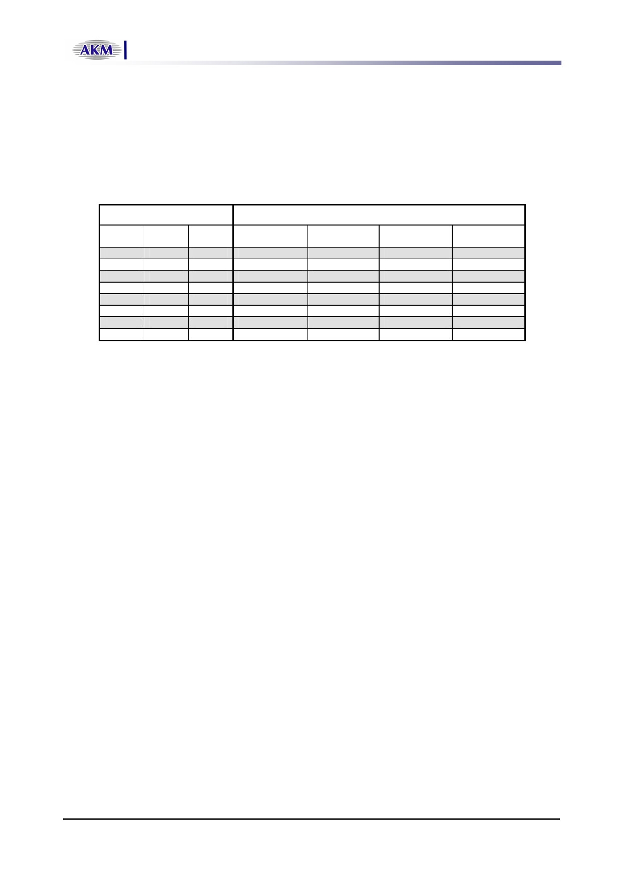
The selectable frequency is shown in Table 1..
Table 1: Clock output Frequency
Selection Pin
Clock Output Frequency (MHz)
S2 S1 S0
CLK1
CLK2
CLK3
(Pin 14) (Pin 3) (Pin 2)
(Pin 7)
(Pin 8)
(Pin 10)
LLL
OFF
OFF
OFF
L LH
OFF
OFF
OFF
LHL
OFF
33.000
OFF
L HH
OFF
33.000
OFF
HL L
OFF
OFF
27.000
HLH
33.000
33.000
OFF
HH L
33.000
33.000
OFF
HHH
33.000
33.000
27.000
* When S2, S1 and S0 are open, the frequency selection is same as “H/H/H”.
* CLK3 and CLK4 are copy of REFOUT.
CLK4
(Pin 11)
OFF
27.000
OFF
27.000
27.000
OFF
27.000
27.000
MS0944-E-00
-5-
Mar-08
5 Page | ||
| Páginas | Total 8 Páginas | |
| PDF Descargar | [ Datasheet AK8131C.PDF ] | |
Hoja de datos destacado
| Número de pieza | Descripción | Fabricantes |
| AK8131C | Multi Clock Generator | AKM |
| Número de pieza | Descripción | Fabricantes |
| SLA6805M | High Voltage 3 phase Motor Driver IC. |
Sanken |
| SDC1742 | 12- and 14-Bit Hybrid Synchro / Resolver-to-Digital Converters. |
Analog Devices |
|
DataSheet.es es una pagina web que funciona como un repositorio de manuales o hoja de datos de muchos de los productos más populares, |
| DataSheet.es | 2020 | Privacy Policy | Contacto | Buscar |
