|
|
|
PDF SIP12109 Data sheet ( Hoja de datos )
| Número de pieza | SIP12109 | |
| Descripción | 4.5 V to 15 V Input Synchronous Buck Regulator | |
| Fabricantes | Vishay | |
| Logotipo | ||
Hay una vista previa y un enlace de descarga de SIP12109 (archivo pdf) en la parte inferior de esta página. Total 18 Páginas | ||
|
No Preview Available !
www.vishay.com
SiP12109
Vishay Siliconix
4 A , 4.5 V to 15 V Input
Synchronous Buck Regulator
DESCRIPTION
The SiP12109 is a high frequency current-mode constant
on-time (CM-COT) synchronous buck regulator with
integrated high-side and low-side power MOSFETs. Its
power stage is capable of supplying 4 A continuous current
at 1.5 MHz switching frequency. This regulator produces an
adjustable output voltage down to 0.6 V from 4.5 V to 15 V
input rail to accommodate a variety of applications,
including computing, consumer electronics, telecom, and
industrial.
SiP12109’s CM-COT architecture delivers ultra-fast
transient response with minimum output capacitance and
tight ripple regulation at very light load. The part is stable
with any capacitor type and no ESR network is required for
loop stability. The device also incorporates a power saving
scheme that significantly increases light load efficiency.
The regulator integrates a full protection feature set,
including output overvoltage protection (OVP), output under
voltage protection (UVP) and thermal shutdown (OTP). It
also has UVLO for input rail and internal soft-start ramp.
The SiP12109 is available in lead (Pb)-free power enhanced
3 mm x 3 mm QFN-16 package.
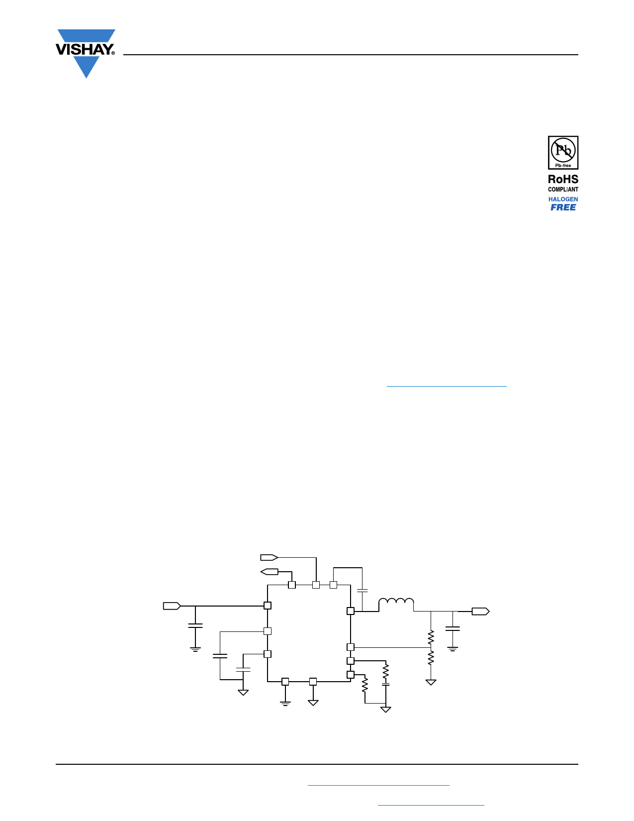
TYPICAL APPLICATION CIRCUIT
FEATURES
• 4.5 V to 15 V input voltage
• Adjustable output voltage down to 0.6 V
• 4 A continuous output current
• Selectable switching frequency from 400 kHz to
1.5 MHz with an external resistor
• 95 % peak efficiency
• Stable with any capacitor. No external ESR network
required
• Ultrafast transient response
• Power saving scheme for increased light load efficiency
• ± 1 % accuracy of VOUT setting
• Cycle-by-cycle current limit
• Fully protected with OTP, SCP, UVP, OVP
• PGOOD Indicator
• -40 °C to +125 °C operating junction temperature
• Output voltage tracking
• Material categorization: For definitions of compliance
please see www.vishay.com/doc?99912
APPLICATIONS
• Point of load regulation for low-power processors,
network processors, DSPs, FPGAs, and ASICs
• Low voltage, distributed power architectures with 5 V
or 12 V rails
• Computing, broadband, networking, LAN/WAN, optical,
test and measurement
• A/V, high density cards, storage, DSL, STB, DVR, DTV,
Industrial PC
INPUT = 4.5 V to 15 V
ENABLE
POWER GOOD
PGOOD EN BOOT
VI N LX
SS
VCC
PG N D
AG N D
VFB
COMP
RO N
VOUT
Fig. 1 - Typical Application Circuit for SiP12109
S13-2479-Rev. A, 16-Dec-13
1
Document Number: 62694
For technical questions, contact: [email protected]
THIS DOCUMENT IS SUBJECT TO CHANGE WITHOUT NOTICE. THE PRODUCTS DESCRIBED HEREIN AND THIS DOCUMENT
ARE SUBJECT TO SPECIFIC DISCLAIMERS, SET FORTH AT www.vishay.com/doc?91000
Free Datasheet http://www.nDatasheet.com
1 page 
www.vishay.com
PIN CONFIGURATION
SiP12109
Vishay Siliconix
VIN 1
VCC 2
AGND 3
RON 4
16 15 14 13
PGND
5 678
12 LX
11 LX
10 LX
9 PGOOD
Fig. 3 - SiP12109 Pin Configuration (Top View)
PIN CONFIGURATION
PIN NUMBER
NAME
1, 16
2
3
4
5
VIN
VCC
AGND
RON
COMP
6 VFB
7 SS
8 EN
9
10, 11, 12
PGOOD
LX
13 BOOT
14, 15, PAD
PGND
FUNCTION
Input supply voltage for power MOS. VIN = 4.5 V to 15 V
Internal regulator output, tie VCC to VIN when VIN is < 5.5 V
Analog ground
An external resistor between RON and AGND sets the switching on time.
Connect to an external RC network for loop compensation and droop function.
Feedback voltage. 0.6 V (typ.). Use a resistor divider between VOUT and AGND to set the output voltage.
An external capacitor between SS and AGND sets the soft start time.
Enable pin. Pull enable above 1.5 V to enable and below 0.4 V to disable the part. Do not float this pin.
Power good output. Open drain.
Switching node, inductor connection point
Bootstrap pin - connect a capacitor of at least 100 nF from BOOT to LX to develop the floating supply
for the high-side gate drive.
Power ground
S13-2479-Rev. A, 16-Dec-13
5
Document Number: 62694
For technical questions, contact: [email protected]
THIS DOCUMENT IS SUBJECT TO CHANGE WITHOUT NOTICE. THE PRODUCTS DESCRIBED HEREIN AND THIS DOCUMENT
ARE SUBJECT TO SPECIFIC DISCLAIMERS, SET FORTH AT www.vishay.com/doc?91000
Free Datasheet http://www.nDatasheet.com
5 Page 
www.vishay.com
SiP12109
Vishay Siliconix
Light Load Operation
To further improve efficiency at light-load condition,
SiP12109 provides a set of innovative implementations to
eliminate LS recirculating current and switching losses. The
internal Zero Crossing Detector (ZCD) monitors LX node
voltage to determine when inductor current starts to flow
negatively. In light load operation as soon as inductor
valley current crosses zero, the device first deploys diode
emulation mode by turning off LS FET. If load further
decreases, switching frequency is further reduced
proportional to load condition to save switching losses while
keeping output ripple within tolerance. The switching
frequency is set by the controller to maintain regulation. At
zero load this frequency can go as low as hundreds of Hz.
OUTPUT MONITORING AND PROTECTION FEATURES
Output Over-Current Protection (OCP)
SiP12109 has pulse-by-pulse over-current limit control. The
inductor valley current is monitored during LS FET turn-on
period through RDS(on) sensing. After a pre-defined time, the
valley current is compared with internal threshold (5 A typ.)
to determine the threshold for OCP. If monitored current is
higher than threshold, HS turn-on pulse is skipped and LS
FET is kept on until the valley current returns below OCP
limit.
In the severe over-current condition, pulse-by-pulse current
limit eventually triggers output under-voltage protection
(UVP), which latches the device off to prevent catastrophic
thermal-related failure. UVP is described in the next section.
OCP is enabled immediately after VCC passes UVLO level.
OCPthreshold
Iload
Iinductor
GH
Skipped GH Pulse
Fig. 22 - Over-Current Protection Illustration
Output Under-Voltage Protection (UVP)
UVP is implemented by monitoring output through VFB pin.
Once the voltage level at VFB is below 0.2 V for more than
20 μs, then UVP event is recognized and both HS and LS
MOSFETs are turned off. UVP latches the device off until
either VCC or EN is recycled.
UVP is only active after the completion of soft-start
sequence.
Output Over-Voltage Protection (OVP)
For OVP implementation, output is monitored through
VFB pin. After soft-start, if the voltage level at VFB is above
21 % (typ.), OVP is triggered with HS FET turning off and
LS FET turning on immediately to discharge the output.
Normal operation is resumed once VFB drops back to
0.675 V.
OVP is active immediately after VCC passes UVLO level.
Over-Temperature Protection (OTP)
SiP12109 has internal thermal monitor block that turns off
both HS and LS FETs when junction temperature is above
160 °C (typ.). A hysteresis of 30 °C is implemented, so when
junction temperature drops below 130 °C, the device
restarts by initiating the soft-start sequence again.
Soft Start up
SiP12109 soft-start time is adjustable by selecting a
capacitor value from the following equation. Once VCC is
above UVLO level (2.55 V typ.), VOUT will ramp up slowly,
rising monotonically to the programmed output voltage.
There is an internal 5 μA current source tied to the soft start
pin which charges the external soft start cap
Cext x 0.8 V
SS time =
5 μA
During soft-start period, OCP is activated. OVP and
short-circuit protection are not active until soft-start is
complete.
S13-2479-Rev. A, 16-Dec-13
11
Document Number: 62694
For technical questions, contact: [email protected]
THIS DOCUMENT IS SUBJECT TO CHANGE WITHOUT NOTICE. THE PRODUCTS DESCRIBED HEREIN AND THIS DOCUMENT
ARE SUBJECT TO SPECIFIC DISCLAIMERS, SET FORTH AT www.vishay.com/doc?91000
Free Datasheet http://www.nDatasheet.com
11 Page | ||
| Páginas | Total 18 Páginas | |
| PDF Descargar | [ Datasheet SIP12109.PDF ] | |
Hoja de datos destacado
| Número de pieza | Descripción | Fabricantes |
| SiP12101 | High Performance Step-Down DC-DC Converter | Vishay |
| SiP12107 | 3A Current-Mode Constant On-Time Synchronous Buck Regulator | Vishay |
| SIP12109 | 4.5 V to 15 V Input Synchronous Buck Regulator | Vishay |
| Número de pieza | Descripción | Fabricantes |
| SLA6805M | High Voltage 3 phase Motor Driver IC. |
Sanken |
| SDC1742 | 12- and 14-Bit Hybrid Synchro / Resolver-to-Digital Converters. |
Analog Devices |
|
DataSheet.es es una pagina web que funciona como un repositorio de manuales o hoja de datos de muchos de los productos más populares, |
| DataSheet.es | 2020 | Privacy Policy | Contacto | Buscar |