|
|
|
PDF K3878 Data sheet ( Hoja de datos )
| Número de pieza | K3878 | |
| Descripción | 900V, 9A, N-channel MOS Field Effect Transistor | |
| Fabricantes | Toshiba | |
| Logotipo | ||
 1. 900V, 9A, MOSFET - 2SK3878 Hay una vista previa y un enlace de descarga de K3878 (archivo pdf) en la parte inferior de esta página. Total 6 Páginas | ||
|
No Preview Available !
2SK3878
TOSHIBA Field Effect Transistor Silicon N-Channel MOS Type (π- MOSIV)
2SK3878
Switching Regulator Applications
• Low drain-source ON-resistance: RDS (ON) = 1.0 Ω (typ.)
• High forward transfer admittance: ⎪Yfs⎪ = 7.0 S (typ.)
• Low leakage current: IDSS = 100 μA (max) (VDS = 720 V)
• Enhancement model: Vth = 2.0 to 4.0 V (VDS = 10 V, ID = 1 mA)
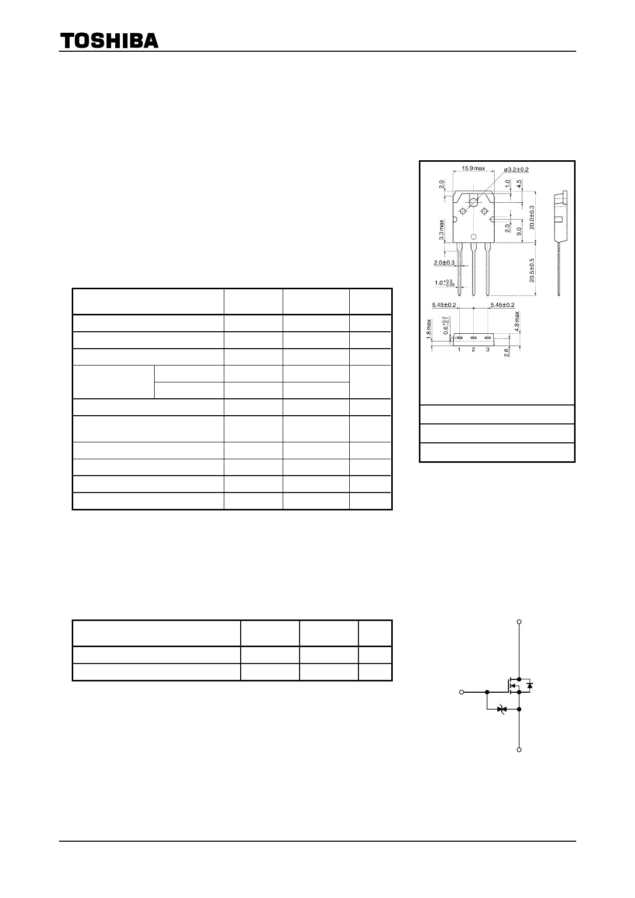
Unit: mm
Absolute Maximum Ratings (Ta = 25°C)
Characteristic
Symbol
Rating
Unit
Drain-source voltage
Drain-gate voltage (RGS = 20 kΩ)
Gate-source voltage
Drain current
DC (Note 1)
Pulse (Note 1)
Drain power dissipation (Tc = 25°C)
Single pulse avalanche energy
(Note 2)
Avalanche current
Repetitive avalanche energy (Note 3)
Channel temperature
Storage temperature range
VDSS
VDGR
VGSS
ID
IDP
PD
EAS
IAR
EAR
Tch
Tstg
900
900
±30
9
27
150
778
9
15
150
−55 to 150
V
V
V
A
W
mJ
A
mJ
°C
°C
1. GATE
2. DRAIN (HEATSINK)
3. SOURCE
JEDEC
―
JEITA
SC-65
TOSHIBA
2−16C1B
Weight: 4.6 g (typ.)
Note: Using continuously under heavy loads (e.g. the application of high temperature/current/voltage and the significant change in
temperature, etc.) may cause this product to decrease in the reliability significantly even if the operating conditions (i.e.
operating temperature/current/voltage, etc.) are within the absolute maximum ratings. Please design the appropriate
reliability upon reviewing the Toshiba Semiconductor Reliability Handbook (“Handling Precautions”/“Derating Concept and
Methods”) and individual reliability data (i.e. reliability test report and estimated failure rate, etc).
Thermal Characteristics
Characteristic
Symbol
Max Unit
Thermal resistance, channel to case
Thermal resistance, channel to ambient
Rth (ch-c)
Rth (ch-a)
0.833
50
°C/W
°C/W
Note 1: Ensure that the channel temperature does not exceed 150°C
during use of the device.
Note 2: VDD = 90 V, Tch = 25°C, L = 17.6 mH, RG = 25 Ω, IAR = 9 A
Note 3: Repetitive rating: pulse width limited by max junction temperature
This transistor is an electrostatic-sensitive device. Handle with care.
1
2
3
1 2010-05-06
Free Datasheet http://www.datasheet4u.com/
1 page 
2SK3878
rth − tw
10
1
Duty = 0.5
0.2
0.1
0.1
0.05
0.02
0.01 0.01
SINGLE PULSE
0.001
10 μ
100 μ
PDM
t
T
Duty = t/T
Rth (ch-c) = 0.833°C/W
1m
10 m
100 m
1
10
PULSE WIDTH tw (s)
SAFE OPERATING AREA
100
ID max (PULSE) *
10 ID max (CONTINUOUS)
1 ms *
100 μs *
DC OPERATION
1 Tc = 25°C
0.1 * SINGLE NONPETITIVE PULSE
Tc = 25°C
Curves must be derated linearly with
increase in temperature.
0.01
1
10 100
VDSS max
1000
10000
DRAIN−SOURCE VOLTAGE VDS (V)
EAS – Tch
1000
800
600
400
200
0
25 50 75 100 125 150
CHANNEL TEMPERATURE (INITIAL) Tch (°C)
15 V
−15 V
BVDSS
IAR
VDD
VDS
TEST CIRCUIT
WAVEFORM
RG = 25 Ω
VDD = 90 V, L = 17.6 mH
ΕAS
=
1
2
⋅
L
⋅I2
⋅
⎜⎜⎝⎛
BVDSS
BVDSS − VDD
⎟⎟⎠⎞
5 2010-05-06
Free Datasheet http://www.datasheet4u.com/
5 Page | ||
| Páginas | Total 6 Páginas | |
| PDF Descargar | [ Datasheet K3878.PDF ] | |
Hoja de datos destacado
| Número de pieza | Descripción | Fabricantes |
| K3870-01 | N-CHANNEL SILICON POWER MOSFET | Fuji |
| K3878 | 900V, 9A, N-channel MOS Field Effect Transistor | Toshiba |
| K3878 | 9A, 900V, N-Channel Power MOSFET | nELL |
| Número de pieza | Descripción | Fabricantes |
| SLA6805M | High Voltage 3 phase Motor Driver IC. |
Sanken |
| SDC1742 | 12- and 14-Bit Hybrid Synchro / Resolver-to-Digital Converters. |
Analog Devices |
|
DataSheet.es es una pagina web que funciona como un repositorio de manuales o hoja de datos de muchos de los productos más populares, |
| DataSheet.es | 2020 | Privacy Policy | Contacto | Buscar |