|
|
|
PDF AOWF12N50 Data sheet ( Hoja de datos )
| Número de pieza | AOWF12N50 | |
| Descripción | 12A N-Channel MOSFET | |
| Fabricantes | Alpha & Omega Semiconductors | |
| Logotipo | ||
Hay una vista previa y un enlace de descarga de AOWF12N50 (archivo pdf) en la parte inferior de esta página. Total 6 Páginas | ||
|
No Preview Available !
AOW12N50/AOWF12N50
500V, 12A N-Channel MOSFET
General Description
Product Summary
The AOW12N50 & AOWF12N50 have been fabricated
using an advanced high voltage MOSFET process that is
designed to deliver high levels of performance and
robustness in popular AC-DC applications.By providing
low RDS(on), Ciss and Crss along with guaranteed avalanche
capability these parts can be adopted quickly into new
and existing offline power supply designs.
VDS
ID (at VGS=10V)
RDS(ON) (at VGS=10V)
100% UIS Tested
100% Rg Tested
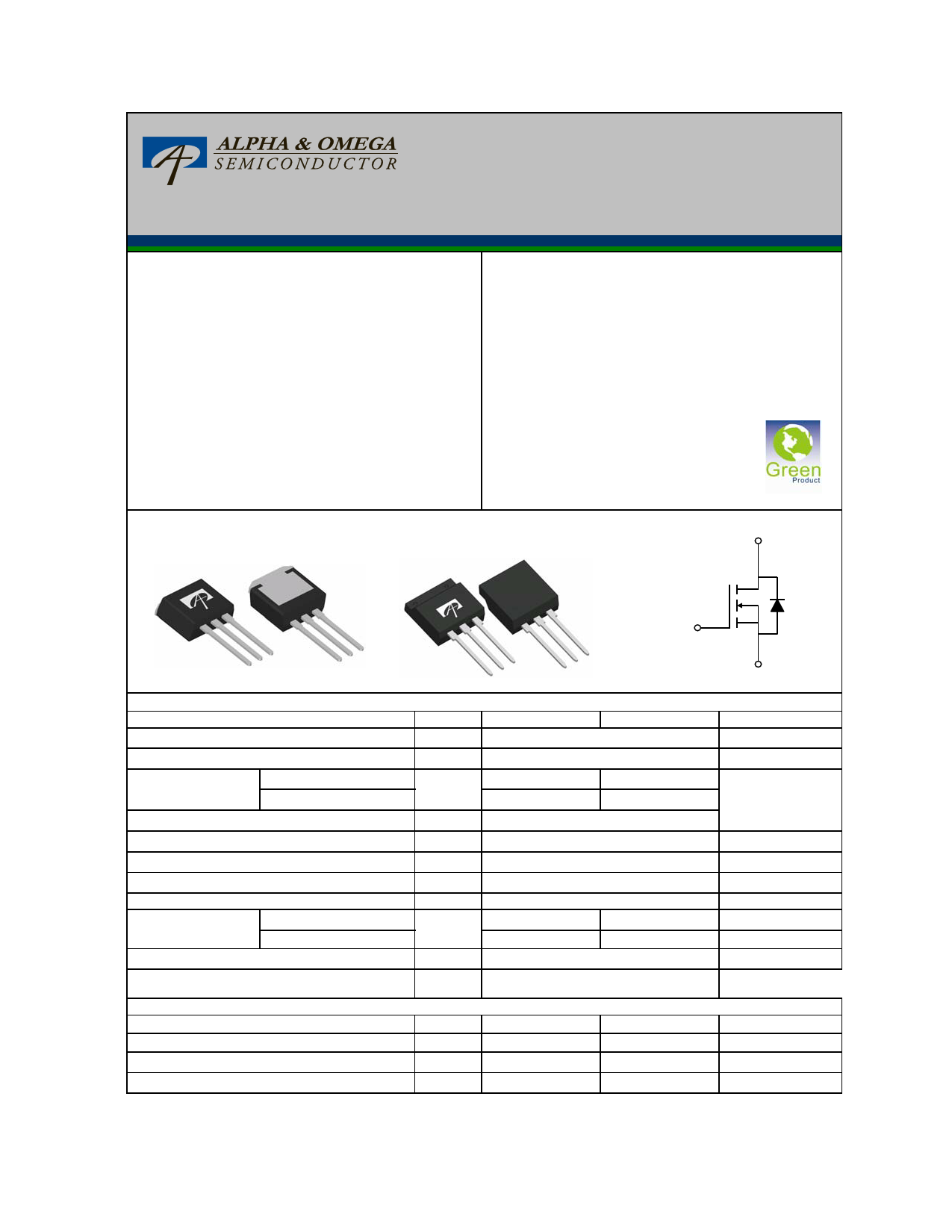
Top View
TO-262
Bottom View
Top View
TO-262F
Bottom View
600V@150℃
12A
< 0.52Ω
D
G DS
G
SD
S
GD
G
SD
G
Absolute Maximum Ratings TA=25°C unless otherwise noted
Parameter
Symbol
AOW12N50
AOWF12N50
Drain-Source Voltage
VDS 500
Gate-Source Voltage
VGS ±30
Continuous Drain
Current
TC=25°C
TC=100°C
ID
12 12*
8.4 8.4*
Pulsed Drain Current C
IDM
48
Avalanche Current C
IAR 5.5
Repetitive avalanche energy C
EAR
454
Single plused avalanche energy G
EAS
908
Peak diode recovery dv/dt
dv/dt
5
TC=25°C
Power Dissipation B Derate above 25oC
PD
250 28
2 0.22
Junction and Storage Temperature Range
Maximum lead temperature for soldering
purpose, 1/8" from case for 5 seconds
TJ, TSTG
TL
-55 to 150
300
Thermal Characteristics
Parameter
Symbol
Maximum Junction-to-Ambient A,D
RθJA
Maximum Case-to-sink A
RθCS
Maximum Junction-to-Case
RθJC
* Drain current limited by maximum junction temperature.
AOW12N50
65
0.5
0.5
AOWF12N50
65
--
4.5
Rev0: June 2010
www.aosmd.com
S
Units
V
V
A
A
mJ
mJ
V/ns
W
W/ oC
°C
°C
Units
°C/W
°C/W
°C/W
Page 1 of 6
Free Datasheet http://www.datasheet4u.com/
1 page 
AOW12N50/AOWF12N50
TYPICAL ELECTRICAL AND THERMAL CHARACTERISTICS
10
D=Ton/T
TJ,PK=TC+PDM.ZθJC.RθJC
RθJC=0.5°C/W
1
In descending order
D=0.5, 0.3, 0.1, 0.05, 0.02, 0.01, single pulse
0.1
0.01
0.00001
Single Pulse
PD
Ton
T
0.0001
0.001
0.01
0.1
1
10
Pulse Width (s)
Figure 12: Normalized Maximum Transient Thermal Impedance for AOW12N50 (Note F)
100
10
D=Ton/T
TJ,PK=TC+PDM.ZθJC.RθJC
1 RθJC=4.5°C/W
In descending order
D=0.5, 0.3, 0.1, 0.05, 0.02, 0.01, single pulse
0.1
0.01
0.001
0.00001
Single Pulse
PD
Ton
T
0.0001
0.001
0.01
0.1
1
10 100
Pulse Width (s)
Figure 13: Normalized Maximum Transient Thermal Impedance for AOWF12N50 (Note F)
1000
Rev0: June 2010
www.aosmd.com
Page 5 of 6
Free Datasheet http://www.datasheet4u.com/
5 Page | ||
| Páginas | Total 6 Páginas | |
| PDF Descargar | [ Datasheet AOWF12N50.PDF ] | |
Hoja de datos destacado
| Número de pieza | Descripción | Fabricantes |
| AOWF12N50 | 12A N-Channel MOSFET | Alpha & Omega Semiconductors |
| Número de pieza | Descripción | Fabricantes |
| SLA6805M | High Voltage 3 phase Motor Driver IC. |
Sanken |
| SDC1742 | 12- and 14-Bit Hybrid Synchro / Resolver-to-Digital Converters. |
Analog Devices |
|
DataSheet.es es una pagina web que funciona como un repositorio de manuales o hoja de datos de muchos de los productos más populares, |
| DataSheet.es | 2020 | Privacy Policy | Contacto | Buscar |