|
|
|
PDF HIP1011D Data sheet ( Hoja de datos )
| Número de pieza | HIP1011D | |
| Descripción | Dual PCI Hot Plug Controller | |
| Fabricantes | Intersil Corporation | |
| Logotipo | ||
Hay una vista previa y un enlace de descarga de HIP1011D (archivo pdf) en la parte inferior de esta página. Total 15 Páginas | ||
|
No Preview Available !
Data Sheet
HIP1011D
November 1999 File Number 4725.1
Dual PCI Hot Plug Controller
The HIP1011D is the first IC available for independent
control of two PCI Hot Plug slots. The HIP1011D has all the
features and functionality of two single PCI Hot Plug slot
controllers such as the HIP1011A but in the same foot print
area.
The HIP1011D is designed to be physically placed in close
proximity to two adjacent PCI slots servicing each
independently but reducing layout complexity and placement
costs in assembly. It creates two independent power control
solutions with discrete power MOSFETs and a few passive
components. The four supplies +5V, +3.3V, +12V, and -12V
for each slot are independently controlled. There are four
integrated current sensing switches for the +12V and -12V
and for the +5V and +3.3V supplies overcurrent protection is
provided by sensing the voltage across external current-
sense resistors. In addition, on-chip references are used to
monitor the +5V, +3.3V and +12V outputs for undervoltage
conditions. The two PWRON inputs control the state of the
switches, one each for slot A and slot B outputs. During an
overcurrent condition on any output, or an undervoltage
condition on the +5V, +3.3V or +12V outputs, a LOW (0V) is
asserted on the associated FLTN output and all associated
switches are latched-off. The outputs servicing the adjacent
slot are unaffected.
The time to FLTN signal going LOW and MOSFET latch off
is user determined by a single capacitor from each FLTN pin
to ground. This added feature enables the HIP1011D to
ignore system noise transients. The FLTN latch is cleared
when the PWRON input is toggled low again. During initial
power-up of the main VCC supply (+12V), the PWRON input
is inhibited from turning on the switches, and the latch is held
in the Reset state until the VCC input is greater than 10V.
User programmability of the overcurrent threshold and turn-
on slew rate is provided. A resistor connected to the OCSET
pin programs the overcurrent threshold for both slots.
Capacitors connected to the gate pins set the turn-on rate.
Features
• Independent Power Control of 2 PCI Slots
• Turn-Off Delay Time Adjustability
• Internal MOSFET Switches for +12V and -12V Outputs
• µP Interface for On/Off Control and Fault Reporting
• Adjustable Overcurrent Protection for All Eight Supplies
• Provides Fault Isolation
• Adjustable Turn-On Slew Rate
• Minimum Parts Count Solution
• No Charge Pump
• 100ns Response Time to Over Current
Applications
• PCI Hot-Plug
Ordering Information
TEMP. RANGE
PART NUMBER
(oC)
PACKAGE
HIP1011DCA
0 to 70 28 Ld SSOP
HIP1011DCA-T
0 to 70 Tape and Reel
PKG.
NO.
M28.15
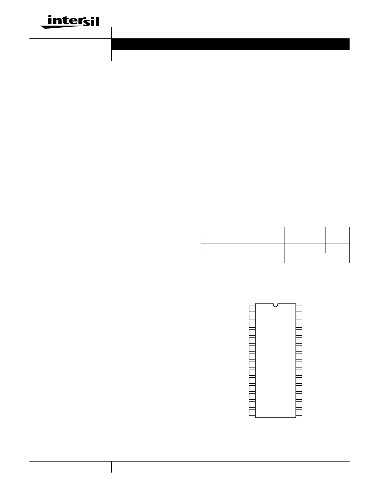
Pinout
HIP1011D
(SSOP)
TOP VIEW
M12VO_2 1
M12VG_2 2
PWRON_2 3
FLTN_2 4
VSS 5
12VG_2 6
12VO_2 7
12VO_1 8
12VG_1 9
OCSET 10
FLTN_1 11
PWRON_1 12
M12VG_1 13
M12VO_1 14
28 M12VIN_2
27 3VISEN_2
26 3VS_2
25 5VISEN_2
24 5VS_2
23 3V5VG_2
22 12VIN_2
21 12VIN_1
20 3V5VG_1
19 5VS_1
18 5VISEN_1
17 3VS_1
16 3VISEN_1
15 M12VIN_1
1 CAUTION: These devices are sensitive to electrostatic discharge; follow proper IC Handling Procedures.
1-888-INTERSIL or 321-724-7143 | Copyright © Intersil Corporation 1999
1 page 
HIP1011D
Absolute Maximum Ratings
12VIN . . . . . . . . . . . . . . . . . . . . . . . . . . . . . . . . . . . . -0.5V to +14.0V
12VO, 12VG, 3V5VG . . . . . . . . . . . . . . . . . . . .-0.5V to 12VIN +0.5V
M12VIN . . . . . . . . . . . . . . . . . . . . . . . . . . . . . . . . . . -14.0V to +0.5V
M12VO, M12VG . . . . . . . . . . . . . . . . . . . . . . VM12VIN-0.5V to +0.5V
3VISEN, 5VISEN . . . . . . . . . . -0.5V to the Lesser of 12VIN or +7.0V
Voltage, Any Other Pin. . . . . . . . . . . . . . . . . . . . . . . . -0.5V to +7.0V
12VO Output Current . . . . . . . . . . . . . . . . . . . . . . . . . . . . . . . . . . .3A
M12VO Output Current . . . . . . . . . . . . . . . . . . . . . . . . . . . . . . . 0.8A
ESD Classification . . . . . . . . . . . . . . . . . . . . . . . . . . . . . 2KeV (HBM)
Thermal Information
Thermal Resistance (Typical, Note 1)
θJA (oC/W)
SSOP Package . . . . . . . . . . . . . . . . . . . . . . . . . . . .
95
Maximum Junction Temperature . . . . . . . . . . . . . . . . . . . . . . .150oC
Maximum Storage Temperature Range . . . . . . . . . . -65oC to 150oC
Maximum Lead Temperature (Soldering 10s) . . . . . . . . . . . . .300oC
(SSOP - Lead Tips Only)
Operating Conditions
12VIN Supply Voltage Range . . . . . . . . . . . . . . . . +10.8V to +13.2V
5V and 3.3V Input Supply Tolerances. . . . . . . . . . . . . . . . . . . . . . ±10%
12VO Output Current . . . . . . . . . . . . . . . . . . . . . . . . . . . . 0 to +0.5A
M12VO Output Current . . . . . . . . . . . . . . . . . . . . . . . . . . 0 to +0.1A
Temperature Range (TA) . . . . . . . . . . . . . . . . . . . . . . . . 0oC to 70oC
CAUTION: Stresses above those listed in “Absolute Maximum Ratings” may cause permanent damage to the device. This is a stress only rating and operation of the
device at these or any other conditions above those indicated in the operational sections of this specification is not implied.
NOTES:
1. θJA is measured with the component mounted on an evaluation PC board in free air.
2. All voltages are relative to GND, unless otherwise specified.
Electrical Specifications Nominal 5.0V and 3.3V Input Supply Voltages,
12VIN = 12V, M12VIN = -12V, TA = TJ = 0 to 70oC, Unless Otherwise Specified
PARAMETER
SYMBOL
TEST CONDITIONS
MIN TYP MAX UNITS
5V/3.3V SUPPLY CONTROL
5V Overcurrent Threshold
5V Overcurrent Threshold Voltage
5V Overcurrent Threshold Voltage
5V Undervoltage Trip Threshold
5V Undervoltage Fault Response Time
5V Turn-On Time
(PWRON High to 5VOUT = 4.75V)
IOC5V
VOC5V_1
VOC5V_2
V5VUV
t5VUV
tON5V
See Figure 24, Typical Application
VOCSET = 0.6V
VOCSET = 1.2V
C3V5VG = 0.022µF, C5VOUT = 2000µF, RL = 1Ω
-
33
70
4.42
-
-
8
42
80
4.65
110
6.5
-
50
90
4.7
160
-
A
mV
mV
V
ns
ms
3V Overcurrent Threshold
3V Overcurrent Threshold Voltage
3V Overcurrent Threshold Voltage
3V Undervoltage Trip Threshold
3V Undervoltage Fault Response Time
3V5VG Undervoltage Enable Threshold
Voltage
IOC3V
See Figure 24, Typical Application
VOC3V_1 VOCSET = 0.6V
VOC3V_2 VOCSET = 1.2V
V3VUV
t3VUV
V3V5VGenVth
- 10 -
41 52 62
89 98 108
2.74 2.86 2.9
- 110 160
- 9.6 -
A
mV
mV
V
ns
V
3V Turn-On Time
(PWRON High to 3VOUT = 3.00V)
3V5VG Vout High
tON3V
C3V5VG = 0.022µF, C3VOUT = 2000µF,
RL = 0.43Ω
Vout_hi_35VG PWRON = High, FLTN = High
- 6.5
11.5 11.8
-
-
ms
V
Gate Output Charge Current
Gate Turn-On Time
(PWRON High to 3V5VG = 11V)
IC3V5VG PWRON = High, V3V+5VG = 4V
19 25.0 29
tON3V5V C3V5VG = 0.033µF, 3V5VG Rising 10% to 90% - 280 -
µA
µs
Gate Turn-Off Time
tOFF3V5V C3V5VG = 0.033µF, 3V5VG Falling 90% to 10%
-
2
- µs
5
5 Page 
HIP1011D
Using the HIP1011DEVAL1 Platform
General and Biasing Information
The HIP1011DEVAL1 platform (Figure 24) comes as a three
part set consisting of 1 mother board emulator and 2 load
cards. This evaluation platform allows a designer to evaluate
and modify the performance and functionality of the
HIP1011D in a simple environment.
Test point numbers (TP#) correspond to the HIP1011D
device (U5) pin numbers thus TP3 and TP12 are PWRON_2
and PWRON_1 respectively. These 2 pins are the HIP1011D
control inputs for each of the 2 integrated but independent
PCI power controllers in the HIP1011D.
On the HIP1011DEVAL1 platform are 4 HUF76132SK8,
(11.5mΩ, 30V, 11.5A) N-Channel power MOSFETs, (Q1-
Q4) these are used as the external switches for the +5V and
+3.3V supplies to the load card connectors, P1 and P2.
Current sensing is facilitated by the four 5mΩ 1W metal strip
resistors (R1-R4), the voltages developed across the sense
resistors are compared to references on board the
HIP1011D.
The HIP1011DEVAL1 platform is powered through the J1 to
J5 connector jacks near the top of the board, see Table 2 for
bias voltage assignments.
TABLE 2. HIP1011DEVAL1 BIAS ASSIGNMENTS
J1 J2 J3 J4 J5
GND
+5V
-12V
+12V
+3.3V
After properly biasing the HIP1011D and ensuring there is
an adequate ground return from the HIP1011DEVAL1
platform to the power supplies, (otherwise anomalous and
unpredictable results will occur) signal the PWRON inputs
low then insert the load cards as shown in Figure 15.
Signaling either or both PWRON pins high (>2.4V) will turn
on the appropriate FET switches and apply voltage to the
load cards.
LOAD CARDS
HIP1011D
Evaluating Time Delay to Latch-Off
Provided for delay to latch-off evaluation are 2 locations for
1206 SMD capacitors, C7 and C8. Filling these locations
places a capacitor to ground from each of the HIP1011D
FLTN pins thus tailoring the FLTN signal going low ramp
rate. This provides a delay to the fault signal latch-off
threshold voltage, FLTN Vth. By increasing this time the
HIP1011D delays immediate latch-off of the bus supply
switches, thus ignoring transient OC and UV conditions. See
Table 3 illustrating the time it takes for switch gate turn-off
from the FLTN start of response to an OC or UV condition.
The FLTN response to an OC or UV condition is 110ns. See
Figures 20 through 23 for waveforms.
The intent of any protection device is to isolate the supply
quickly so a faulty card does not drag down a supply. A
longer latch-off delay results in less isolation from a faulty
card to supply.
TABLE 3.
C7 AND C8 VALUE OPEN 0.001µF 0.01µF 0.1µF
FLTN to Gate Response 0.1µs 0.44µs 2.9µs 28µs
FLTN
3V5VG
FLTN, Vth
FIGURE 16. TIMING DIAGRAM
10ms
1ms
100µs
10µs
1µs
100ns
10ns
1ns
OPEN
0.001µF
0.01µF
0.1µF
1µF 10µF
FIGURE 17. TYPICAL OC/UV TO VG RESPONSE vs FLTN CAP
FIGURE 15. cORRECT INSTALLATION OF LOAD CARDS
11
11 Page | ||
| Páginas | Total 15 Páginas | |
| PDF Descargar | [ Datasheet HIP1011D.PDF ] | |
Hoja de datos destacado
| Número de pieza | Descripción | Fabricantes |
| HIP1011 | PCI Hot Plug Controller | Intersil Corporation |
| HIP1011A | PCI Hot Plug Controller | Intersil Corporation |
| HIP1011B | PCI Hot Plug Controller | Intersil Corporation |
| HIP1011D | Dual PCI Hot Plug Controller | Intersil Corporation |
| Número de pieza | Descripción | Fabricantes |
| SLA6805M | High Voltage 3 phase Motor Driver IC. |
Sanken |
| SDC1742 | 12- and 14-Bit Hybrid Synchro / Resolver-to-Digital Converters. |
Analog Devices |
|
DataSheet.es es una pagina web que funciona como un repositorio de manuales o hoja de datos de muchos de los productos más populares, |
| DataSheet.es | 2020 | Privacy Policy | Contacto | Buscar |