|
|
|
PDF IS31AP2006 Data sheet ( Hoja de datos )
| Número de pieza | IS31AP2006 | |
| Descripción | 3W MONO FILTER-LESS CLASS-D AUDIO POWER AMPLIFIER | |
| Fabricantes | ISSI | |
| Logotipo | ||
Hay una vista previa y un enlace de descarga de IS31AP2006 (archivo pdf) en la parte inferior de esta página. Total 14 Páginas | ||
|
No Preview Available !
IS31AP2006
3W MONO FILTER-LESS CLASS-D AUDIO POWER AMPLIFIER
April 2012
GENERAL DESCRIPTION
The IS31AP2006 is a high efficiency, 3W mono
Class-D audio power amplifier. A low noise, filter-less
PWM architecture eliminates the output filter, reducing
external component count, system cost, and
simplifying design.
Operating in a single 5V supply, IS31AP2006 is
capable of driving 4Ω speaker load at a continuous
average output of 3W with 10% THD+N. The
IS31AP2006 has high efficiency with speaker load
compared to a typical class-AB amplifier.
In cellular handsets, the earpiece, speaker phone, and
melody ringer can each be driven by the IS31AP2006.
The gain of IS31AP2006 is externally configurable
which allows independent gain control from multiple
sources by summing signals from each function.
The IS31AP2006 is available in DFN-8 (3mm×3mm)
packages.
FEATURES
5V supply at THD = 10%
-3W into 4Ω (Typ.)
-1.70W into 8Ω (Typ.)
Efficiency at 5V:
-83% at 400mW with a 4Ω speaker
-89% at 400mW with an 8Ω speaker
Optimized PWM output stage eliminates LC
output filter
Fully differential design reduces RF rectification
and eliminates bypass capacitor
Integrated pop-and-click suppression circuitry
DFN-8 (3mm×3mm) packages
APPLICATIONS
Wireless or cellular handsets and PDAs
Portable DVD player
Notebook PC
Portable radio
Educational toys
USB speakers
Portable gaming
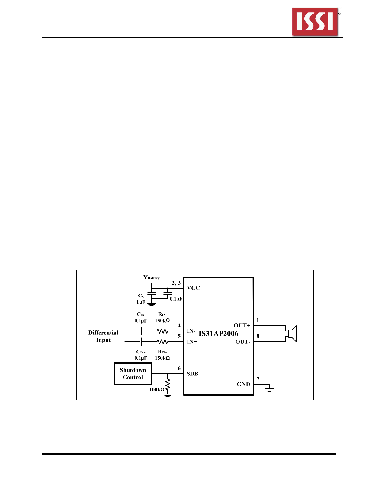
TYPICAL APPLICATION CIRCUIT
http://www.DataSheet4U.net/
Figure 1 Typical Application Circuit (Differential Input)
Integrated Silicon Solution, Inc. – www.issi.com
Rev.A, 03/27/2012
1
datasheet pdf - http://www.DataSheet4U.net/
1 page 
IS31AP2006
ABSOLUTE MAXIMUM RATINGS
Supply voltage, VCC
Voltage at any input pin
Maximum junction temperature, TJMAX
Storage temperature range, TSTG
Operating temperature range, TA
ESD HBM
-0.3V ~ +6.0V
-0.3V ~ VCC+0.3V
150°C
-65°C ~ +150°C
−40°C ~ +85°C
7kV
Note:
Stresses beyond those listed under “Absolute Maximum Ratings” may cause permanent damage to the device. These are stress ratings only and
functional operation of the device at these or any other condition beyond those indicated in the operational sections of the specifications is not
implied. Exposure to absolute maximum rating conditions for extended periods may affect device reliability.
ELECTRICAL CHARACTERISTICS
VCC = 2.7V ~ 5.5V, TA = 25°C, unless otherwise noted.
Symbol
Parameter
Condition
VCC Supply voltage
VOS
Output offset voltage
(measured differentially)
ICC Quiescent current
ISD
fsw
RIN
Gain
VIH
VIL
Shutdown current
Switching frequency
Input resistor
Input gain
High-level input voltage
Low-level input voltage
VSDB = 0V, AV = 2V/V
VCC = 5.5V, no load
VCC = 2.7V, no load
VSDB = 0.4V
Gain 20V/V
RIN = 150kΩ
http://www.DataSheet4U.net/
Min.
2.7
Typ.
Max.
5.5
Unit
V
10 mV
2.6
mA
1.2
1 μA
250 kHz
15 kΩ
2 V/V
1.4 V
0.4 V
Integrated Silicon Solution, Inc. – www.issi.com
Rev.A, 03/27/2012
5
datasheet pdf - http://www.DataSheet4U.net/
5 Page 
IS31AP2006
INPUT CAPACITORS (CIN)
The input capacitors and input resistors form a
high-pass filter with the corner frequency, fC,
determined in equation (2).
1
fc 2RIN CIN
(2)
The value of the input capacitor is important to
consider as it directly affects the bass (low frequency)
performance of the circuit. Speakers in wireless
phones cannot usually respond well to low frequencies,
so the corner frequency can be set to block low
frequencies in this application.
Equation (3) is reconfigured to solve for the input
coupling capacitance.
1
CIN 2RIN fc
(3)
If the corner frequency is within the audio band, the
capacitors should have a tolerance of 10% or better,
because any mismatch in capacitance causes an
impedance mismatch at the corner frequency and
below.
For a flat low-frequency response, use large input
coupling capacitors (1μF). However, in a GSM phone
the ground signal is fluctuating at 217Hz, but the signal
from the codec does not have the same 217Hz
fluctuation. The difference between the two signals is
amplified, sent to the speaker, and heard as a 217Hz
hum.
SUMMING INPUT SIGNALS
Most wireless phones or PDAs need to sum signals at
the audio power amplifier or just have two signal
sources that need separate gain. The IS31AP2006
makes it easy to sum signals or use separate signal
sources with different gains. Many phones now use the
same speaker for the earpiece and ringer, where the
wireless phone would require a much lower gain for
the phone earpiece than for the ringer. PDAs and
phones that have stereo headphones require summing
of the right and left channels to output the stereo signal
to the mono speaker.
SUMMING TWO DIFFERENTIAL INPUT SIGNALS
Two extra resistors are needed for summing
differential signals. The gain for each input source can
be set independently (see equations (4) and (5), and
Figure 14).
Gain1 2 150k V
RIN1 V
Gain 2 2 150k V
RIN 2 V
(4)
(5)
Figure 14 Application Circuit with Summing Two Differential Inputs
If summing left and right inputs with a gain of 1V/V, use
RIN1 = RIN2 = 300kΩ.
If summing a ring tone and a phone signal, set the
ring-tone gain to Gain2 = 2V/V, and the phone gain to
Gain1 = 0.1V/V. The resistor values would be.
RIN1 = 3MΩ, and RIN2 = 150kΩ.
SUMMING A DIFFERENTIAL INPUT SIGNAL AND A
SINGLE-ENDED INPUT SIGNAL
Figure 15 shows how to sum a differential input signal
and a single-ended input signal. Ground noise may
couple in through IN- with this method. It is better to
use differential inputs. The corner frequency of the
single-ended input is set by CIN2, shown in equation (8).
To assure that each input is balanced, the
single-ended input must be driven by a low-impedance
source even if the input is not in use.
http://www.DataSheet4U.net/
Gain1 2 150k V
RIN1 V
(6)
Gain2 2 150k V
RIN 2 V
(7)
1
CIN 2 2RIN 2 fc 2
(8)
If summing a ring tone and phone signals, the phone
signals should use the differential inputs while the ring
tone should use the single-ended input. The phone
gain is set at Gain2 = 0.1V/V, and the ring-tone gain is
set to Gain2 = 0.1V/V, the resistor values would be
RIN1 = 150kΩ, and RIN2 = 3MΩ
The high pass corner frequency of the single-ended
input is set by CIN2. If the desired corner frequency is
less than 20Hz.
1
CIN1 2RIN1 fC1
C IN 2 53 pF
(9)
(10)
Integrated Silicon Solution, Inc. – www.issi.com
Rev.A, 03/27/2012
11
datasheetpdf-http://www.DataSheet4U.net/
11 Page | ||
| Páginas | Total 14 Páginas | |
| PDF Descargar | [ Datasheet IS31AP2006.PDF ] | |
Hoja de datos destacado
| Número de pieza | Descripción | Fabricantes |
| IS31AP2005 | 2.95W MONO FILTER-LESS CLASS-D AUDIO POWER AMPLIFIER | ISSI |
| IS31AP2006 | 3W MONO FILTER-LESS CLASS-D AUDIO POWER AMPLIFIER | ISSI |
| Número de pieza | Descripción | Fabricantes |
| SLA6805M | High Voltage 3 phase Motor Driver IC. |
Sanken |
| SDC1742 | 12- and 14-Bit Hybrid Synchro / Resolver-to-Digital Converters. |
Analog Devices |
|
DataSheet.es es una pagina web que funciona como un repositorio de manuales o hoja de datos de muchos de los productos más populares, |
| DataSheet.es | 2020 | Privacy Policy | Contacto | Buscar |