|
|
PDF ISL9112 Data sheet ( Hoja de datos )
| Número de pieza | ISL9112 | |
| Descripción | (ISL9110 / ISL9112) 1.2A High Efficiency Buck-Boost Regulators | |
| Fabricantes | Intersil Corporation | |
| Logotipo |  |
|
Hay una vista previa y un enlace de descarga de ISL9112 (archivo pdf) en la parte inferior de esta página. Total 20 Páginas | ||
|
No Preview Available !
1.2A High Efficiency Buck-Boost Regulators
ISL9110, ISL9112
The ISL9110 and ISL9112 are highly-integrated Buck-Boost
switching regulators that accept input voltages either above or
below the regulated output voltage. Unlike other Buck-Boost
regulators, these regulators automatically transition between
operating modes without significant output disturbance.
Both parts are capable of delivering up to 1.2A output current,
and provide excellent efficiency due to their fully synchronous
4-switch architecture. No-load quiescent current of only 35µA
also optimizes efficiency under light-load conditions. Forced
PWM and/or synchronization to an external clock may also be
selected for noise sensitive applications.
The ISL9110 is designed for standalone applications and
supports 3.3V and 5V fixed output voltages or variable output
voltages with an external resistor divider. Output voltages as low
as 1V, or as high as 5.2V are supported using an external resistor
divider.
The ISL9112 supports a broader set of programmable features
that may be accessed via an I2C bus interface. With a
programmable output voltage range of 1.9V to 5V, the ISL9112
is ideal for applications requiring dynamically changing supply
voltages. A programmable slew rate can be selected to provide
smooth transitions between output voltage settings.
The ISL9110 and ISL9112 require only a single inductor and very
few external components. Power supply solution size is
minimized by a tiny 3mmx3mm package and a 2.5MHz
switching frequency, which further reduces the size of external
components.
Features
• Accepts Input Voltages Above or Below Regulated Output
Voltage
• Automatic and Seamless Transitions Between Buck and Boost
Modes
• Input Voltage Range: 1.8V to 5.5V
• Output Current: Up to 1.2A
• High Efficiency: Up to 95%
• 35µA Quiescent Current Maximizes Light-load Efficiency
• 2.5MHz Switching Frequency Minimizes External Component
Size
• Selectable Forced-PWM Mode and External Synchronization
• I2C Interface (ISL9112)
• Fully Protected for Overcurrent, Over-temperature and
Undervoltage
• Small 3mmx3mm TDFN Package
Applications
• Regulated 3.3V from a Single Li-Ion Battery
• Smart Phones and Tablet Computers
• Handheld Devices
• Point-of-Load Regulators
Related Literature
• See AN1648 “ISL9110IRTNEVAL1Z, ISL9110IRT7EVAL1Z,
ISL9110IRTAEVAL1Z Evaluation Board User Guide”
• See AN1647 “ISL9112IRTNEVAL1Z, ISL9112IRT7EVAL1Z
EvaluationBoard User Guide”
VIN =
1.8V TO 5.5V
C1
10µF
STATUS
OUTPUTS
ISL9110IRTNZ
5 PVIN
LX1 4
6
10
9
8
7
VIN
MODE
EN
BAT
PG
LX2
VOUT
2
1
FB 12
L1
2.2µH
VOUT =
3.3V/1A
C2
10µF
FIGURE 1. TYPICAL APPLICATION
100
95
90
VIN = 5V
85
80 VIN = 3V
75
VOUT = 3.3V
70
0.01
VIN = 2.5V
0.05
IOUT (A)
0.25
FIGURE 2. EFFICIENCY
1.25
July 13, 2012
FN7649.2
1
CAUTION: These devices are sensitive to electrostatic discharge; follow proper IC Handling Procedures.
1-888-INTERSIL or 1-888-468-3774 |Copyright Intersil Americas Inc. 2011, 2012. All Rights Reserved
Intersil (and design) is a trademark owned by Intersil Corporation or one of its subsidiaries.
All other trademarks mentioned are the property of their respective owners.
1 page 
ISL9110, ISL9112
Absolute Maximum Ratings
PVIN, VIN . . . . . . . . . . . . . . . . . . . . . . . . . . . . . . . . . . . . . . . . . . . -0.3V to 6.5V
LX1, LX2 (Note 7) . . . . . . . . . . . . . . . . . . . . . . . . . . . . . . . . . . . . -0.3V to 6.5V
FB (adjustable version) . . . . . . . . . . . . . . . . . . . . . . . . . . . . . . . -0.3V to 2.7V
FB (fixed VOUT versions) . . . . . . . . . . . . . . . . . . . . . . . . . . . . . . . -0.3V to 6.5V
GND, PGND . . . . . . . . . . . . . . . . . . . . . . . . . . . . . . . . . . . . . . . . . -0.3V to 0.3V
All Other Pins . . . . . . . . . . . . . . . . . . . . . . . . . . . . . . . . . . . . . . . -0.3V to 6.5V
ESD Rating
Human Body Model (Tested per JESD22-A114E) . . . . . . . . . . . . . . . . 3kV
Machine Model (Tested per JESD22-A115-A) . . . . . . . . . . . . . . . . . 250V
Latch Up (Tested per JESD-78B; Class 2, Level A) . . . . . . . . . . . . . . 100mA
Thermal Information
Thermal Resistance (Typical)
θJA (°C/W) θJC (°C/W)
12 Ld TDFN Package (Notes 5, 6) . . . . . . .
42
5.5
Maximum Junction Temperature (Plastic Package) . . . . . . . . . . . .+125°C
Storage Temperature Range. . . . . . . . . . . . . . . . . . . . . . . .-65°C to +150°C
Pb-Free Reflow Profile . . . . . . . . . . . . . . . . . . . . . . . . . . . . . . . see link below
http://www.intersil.com/pbfree/Pb-FreeReflow.asp
Recommended Operating Conditions
Temperature Range . . . . . . . . . . . . . . . . . . . . . . . . . . . . . . . . -40°C to +85°C
Supply Voltage Range . . . . . . . . . . . . . . . . . . . . . . . . . . . . . . . . . 1.8V to 5.5V
Load Current Range . . . . . . . . . . . . . . . . . . . . . . . . . . . . . . . . . . . . 0A to 1.2A
CAUTION: Do not operate at or near the maximum ratings listed for extended periods of time. Exposure to such conditions may adversely impact product
reliability and result in failures not covered by warranty.
NOTES:
5. θJA is measured in free air with the component mounted on a high effective thermal conductivity test board with “direct attach” features. See Tech
Brief TB379
6. For θJC, the “case temp” location is the center of the exposed metal pad on the package underside.
7. LX1 and LX2 pins can withstand switching transients of -1.5V for 100ns, and 7V for 20ms.
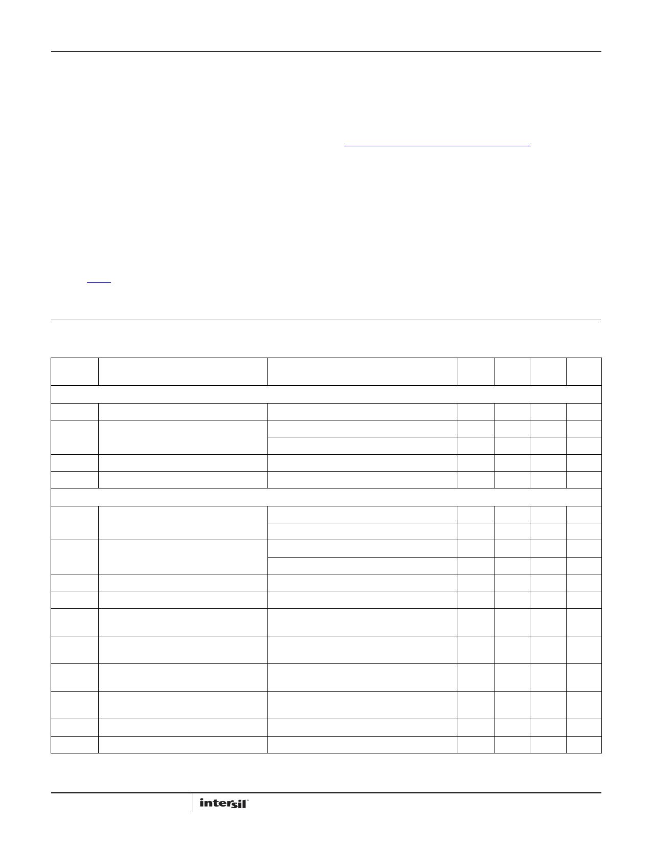
Analog Specifications VVIN = VPVIN = VEN = 3.6V, VOUT = 3.3V, L1 = 2.2µH, C1 = C2 = 10µF, TA = +25°C. Boldface limits apply over the
operating temperature range, -40°C to +85°C.
SYMBOL
PARAMETER
TEST CONDITIONS
MIN TYP MAX
(Note 8) (Note 9) (Note 8) UNITS
POWER SUPPLY
VIN
VUVLO
Input Voltage Range
VIN Undervoltage Lockout Threshold
Rising
Falling
1.8
1.550
1.725
1.650
5.5
1.775
V
V
V
IVIN VIN Supply Current
ISD VIN Supply Current, Shutdown
OUTPUT VOLTAGE REGULATION
PFM mode, no external load on Vout (Note 10)
EN = GND, VIN = 3.6V
35
0.05
60
1.0
µA
µA
VOUT Output Voltage Range
Output Voltage Accuracy
VFB
IFB
ΔVOUT /
ΔVIN
ΔVOUT /
ΔIOUT
ΔVOUT /
ΔVI
ΔVOUT /
ΔIOUT
VCLAMP
FB Pin Voltage Regulation
FB Pin Bias Current
Line Regulation, PWM Mode
Load Regulation, PWM Mode
Line Regulation, PFM Mode
Load Regulation, PFM Mode
Output Voltage Clamp
Output Voltage Clamp Hysteresis
ISL9110IRTAZ, IOUT = 100mA
ISL9112, IOUT = 100mA
VIN = 3.7V, VOUT = 3.3V, IOUT = 0mA, PWM mode
VIN = 3.7V, VOUT = 3.3V, IOUT = 1mA, PFM mode
For adjustable output version
For adjustable output version
IOUT = 500mA, VOUT = 3.3V, MODE = GND, VIN step
from 2.3V to 5.5V
VIN = 3.7V, VOUT = 3.3V, MODE = GND, IOUT step
from 0mA to 500mA
IOUT = 100mA, VOUT = 3.3V, MODE = VIN, VIN step
from 2.3V to 5.5V
VIN=3.7V, VOUT = 3.3V, MODE = VIN, IOUT step from
0mA to 100mA
Rising, VIN = 3.6V
VIN = 3.6V
1.00
1.90
-2
-3
0.79
5.25
0.80
±0.005
±0.005
±12.5
±0.4
400
5.20
5.00
+2
+4
0.81
1
5.95
V
V
%
%
V
µA
mV/mV
mV/mA
mV/V
mV/mA
V
mV
5 FN7649.2
July 13, 2012
5 Page 
ISL9110, ISL9112
Typical Performance Curves (Continued)
LX1
2V/DIV
VIN = 4V
VOUT = 3.3V
IOUT = 200mA
LX2
2V/DIV
LX1
2V/DIV
VIN = 2V
VOUT = 3.3V
IOUT = 200mA
LX2
2V/DIV
VOUT
2V/DIV
EN
2V/DIV
400µs/DIV
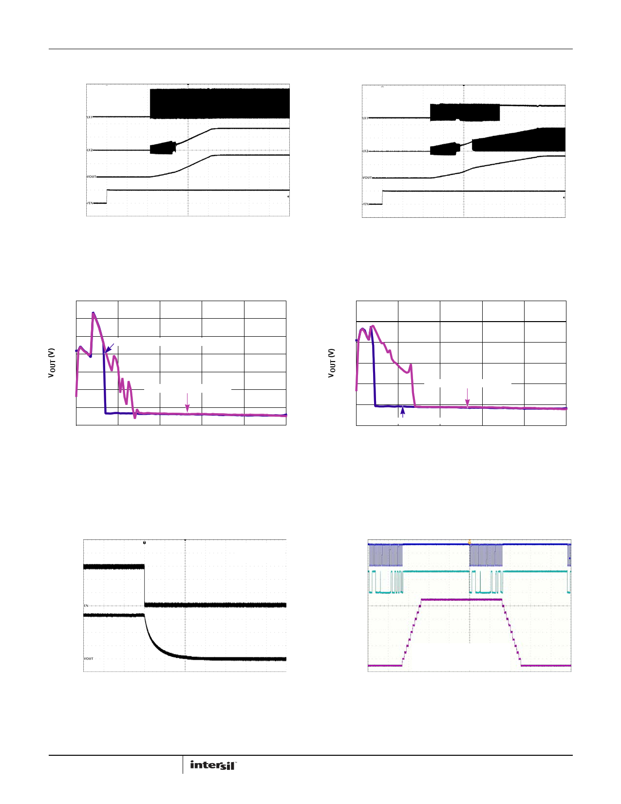
FIGURE 21. SOFT-START, VIN = 4V, VOUT = 3.3V
VOUT
2V/DIV
EN
2V/DIV
400µs/DIV
FIGURE 22. SOFT-START, VIN = 2V, VOUT = 3.3V
3.315
3.310
3.305
3.300
LOAD CURRENT FALLING
3.295
3.290
LOAD CURRENT RISING
3.285
3.280
0.0 0.1 0.2 0.3 0.4 0.5
IOUT (mA)
FIGURE 23. OUTPUT VOLTAGE vs LOAD CURRENT
(VIN = 2.5V, VOUT = 3.3V, AUTO PFM/PWM MODE)
3.310
3.305
3.300
3.295
3.290
LOAD CURRENT RISING
3.285
3.2800.0LOAD
CURRENT
0.1
FALLING
0.2
0.3
0.4
0.5
IOUT (mA)
FIGURE 24. OUTPUT VOLTAGE vs LOAD CURRENT
(VIN = 4.5V, VOUT = 3.3V, AUTO PFM/PWM MODE)
EN
1V/DIV
VIN = 3.7V
VOUT = 3.3V
VOUT
1V/DIV
4ms/DIV
FIGURE 25. OUTPUT SOFT-DISCHARGE
SCL
2V/DIV
SDA
2V/DIV
VOUT
200mV/DIV
VIN = 5V
VOUT = 3.0V → 4.0V → 3.0V
SLEWRATE = 0b111
1ms/DIV
FIGURE 26. DIGITAL SLEW OPERATION (ISL9112)
11 FN7649.2
July 13, 2012
11 Page | ||
| Páginas | Total 20 Páginas | |
| PDF Descargar | [ Datasheet ISL9112.PDF ] | |
Hoja de datos destacado
| Número de pieza | Descripción | Fabricantes |
| ISL9110 | (ISL9110 / ISL9112) 1.2A High Efficiency Buck-Boost Regulators | Intersil Corporation |
| ISL91106 | High Efficiency High Current Buck-Boost Regulator | Intersil |
| ISL91106A | High Efficiency High Current Buck-Boost Regulator | Intersil |
| ISL91107 | High Efficiency Buck-boost Regulator | Intersil |
| Número de pieza | Descripción | Fabricantes |
| SLA6805M | High Voltage 3 phase Motor Driver IC. |
Sanken |
| SDC1742 | 12- and 14-Bit Hybrid Synchro / Resolver-to-Digital Converters. |
Analog Devices |
|
DataSheet.es es una pagina web que funciona como un repositorio de manuales o hoja de datos de muchos de los productos más populares, |
| DataSheet.es | 2020 | Privacy Policy | Contacto | Buscar |
