|
|
|
PDF HD74LV1GW97A Data sheet ( Hoja de datos )
| Número de pieza | HD74LV1GW97A | |
| Descripción | Configurable Multiple-Function Gate | |
| Fabricantes | Renesas Technology | |
| Logotipo | ||
Hay una vista previa y un enlace de descarga de HD74LV1GW97A (archivo pdf) en la parte inferior de esta página. Total 9 Páginas | ||
|
No Preview Available !
HD74LV1GW97A
Configurable Multiple–Function Gate
REJ03D0083-0300
Rev.3.00
May 19, 2006
www.DatDaSehesetc4Ur.nipet tion
The HD74LV1GW97A has configurable multiple–function gate in a 6 pin package. The Output state is determined by
eight patterns of 3–bit input. The user can choose the logic functions AND, NAND, OR, NOR, INVERTER, Non–
Invert Buffer, Data Selector. Low voltage and high-speed operation is suitable for the battery powered products (e.g.,
notebook computers), and the low power consumption extends the battery life.
Features
• The basic gate function is lined up as Renesas uni logic series.
• Supplied on emboss taping for high-speed automatic mounting.
• Supply voltage range : 1.65 to 5.5 V
Operating temperature range : –40 to +85°C
• All inputs VIH (Max.) = 5.5 V (@VCC = 0 V to 5.5 V)
All outputs VO (Max.) = 5.5 V (@VCC = 0 V)
• Output current ±6 mA (@VCC = 3.0 V to 3.6 V), ±12 mA (@VCC = 4.5 V to 5.5 V)
• All the logical input has hysteresis voltage for the slow transition.
• Ordering Information
Part Name
Package Type
Package Code
(Previous Code)
Package
Abbreviation
HD74LV1GW97ACME CMPAK-6 pin
PTSP0006JA-A
(CMPAK-6V)
CM
Taping
Abbreviation (Quantity)
E (3,000 pcs / Reel)
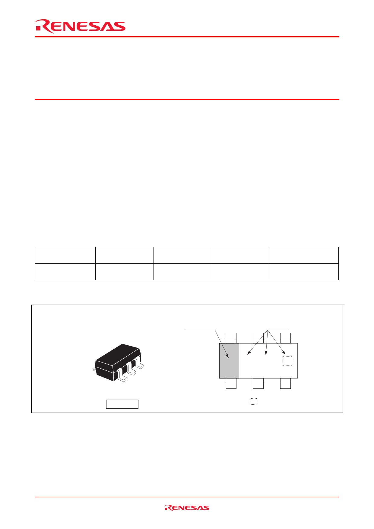
Outline and Article Indication
• HD74LV1GW97A
Index band
Marking
W2
CMPAK–6
= Control code
Rev.3.00, May 19, 2006 page 1 of 8
1 page 
HD74LV1GW97A
Electrical Characteristics
Ta = –40 to 85°C
Item
Symbol
VT+
VCC (V)
1.65 to 1.95
2.5
3.3
Min
—
—
—
Typ Max Unit
— VCC×0.75
— 1.75
— 2.31
Test condition
5.0 — — 3.50
Threshold
voltage
1.65 to 1.95 VCC×0.25
—
VT–
2.5 0.75 —
3.3 0.99 —
—
—
V
—
5.0 1.5 — —
1.65 to 1.95
0.1
2.5 0.25
∆VT 3.3 0.33
— VCC×0.4
— 1.0
— 1.32
5.0 0.5 — 2.0
Output voltage
Input current
Quiescent
supply current
Output leakage
current
Min to Max VCC–0.1
—
1.65 1.4 —
VOH 2.3 2.0 —
3.0 2.48 —
4.5 3.8 —
Min to Max
—
—
1.65 — —
VOL 2.3
——
3.0 — —
4.5 — —
IIN 0 to 5.5 — —
ICC 5.5 — —
IOFF
0
——
—
—
—
—
—
0.1
0.3
0.4
0.44
0.55
±1
10
5
IOH = –50 µA
IOH = –1 mA
IOH = –2 mA
IOH = –6 mA
V IOH = –12 mA
IOL = 50 µA
IOL = 1 mA
IOL = 2 mA
IOL = 6 mA
IOL = 12 mA
µA VIN = 5.5 V or GND
µA
VIN = VCC or GND,
IO = 0
µA VIN or VO = 0 to 5.5 V
Input capacitance
CIN
3.3
— 3.0 — pF VIN = VCC or GND
Note: For conditions shown as Min or Max, use the appropriate values under recommended operating conditions.
Rev.3.00, May 19, 2006 page 5 of 8
5 Page | ||
| Páginas | Total 9 Páginas | |
| PDF Descargar | [ Datasheet HD74LV1GW97A.PDF ] | |
Hoja de datos destacado
| Número de pieza | Descripción | Fabricantes |
| HD74LV1GW97A | Configurable Multiple-Function Gate | Renesas Technology |
| Número de pieza | Descripción | Fabricantes |
| SLA6805M | High Voltage 3 phase Motor Driver IC. |
Sanken |
| SDC1742 | 12- and 14-Bit Hybrid Synchro / Resolver-to-Digital Converters. |
Analog Devices |
|
DataSheet.es es una pagina web que funciona como un repositorio de manuales o hoja de datos de muchos de los productos más populares, |
| DataSheet.es | 2020 | Privacy Policy | Contacto | Buscar |