|
|
|
PDF IRF7342PBF Data sheet ( Hoja de datos )
| Número de pieza | IRF7342PBF | |
| Descripción | Power MOSFET ( Transistor ) | |
| Fabricantes | International Rectifier | |
| Logotipo | ||
Hay una vista previa y un enlace de descarga de IRF7342PBF (archivo pdf) en la parte inferior de esta página. Total 7 Páginas | ||
|
No Preview Available !
PD - 95200
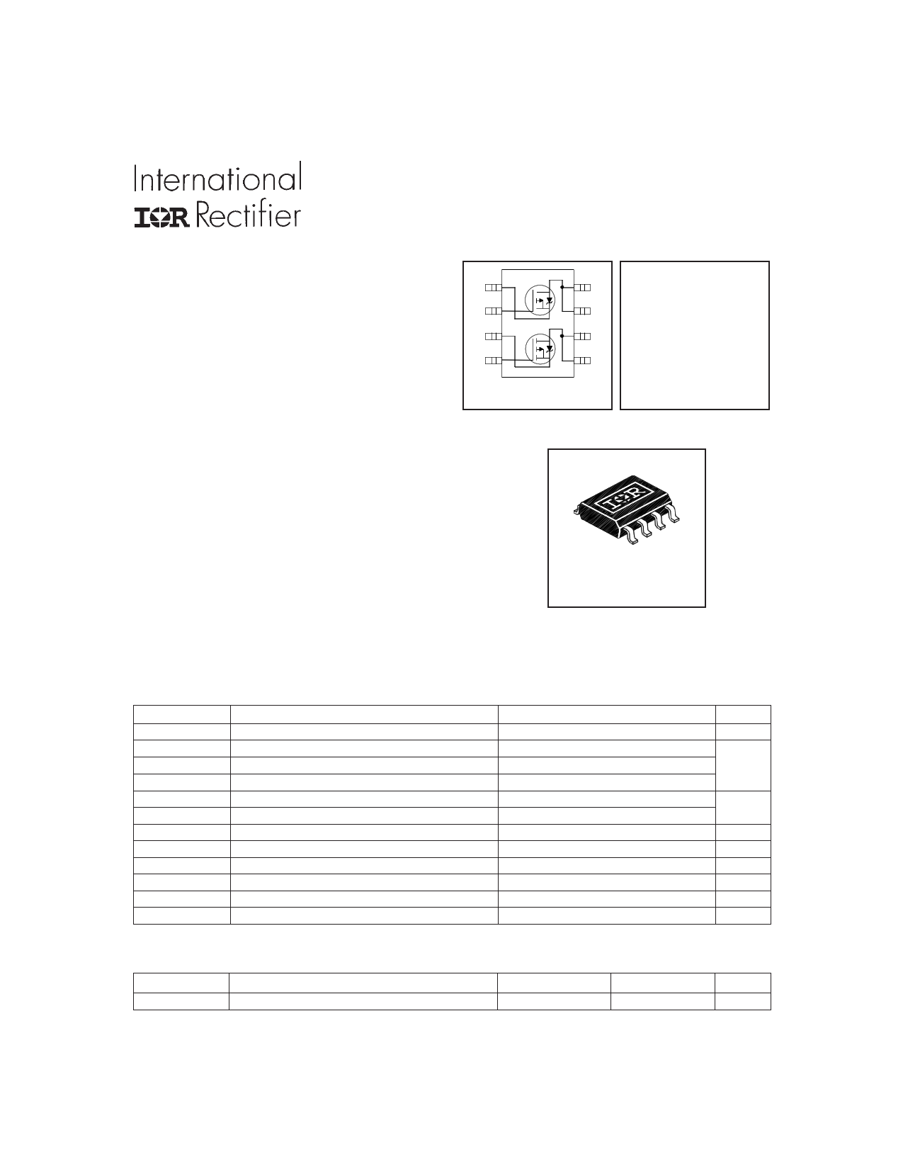
IRF7342PbF
l Generation V Technology
HEXFET® Power MOSFET
l Ultra Low On-Resistance
l Dual P-Channel Mosfet
l Surface Mount
l Available in Tape & Reel
l Dynamic dv/dt Rating
l Fast Switching
l Lead-Free
Description
S1 1
G1 2
8 D1
7 D1
VDSS = -55V
S2 3
6 D2
G2 4
5 D2 RDS(on) = 0.105Ω
Top View
Fifth Generation HEXFETs from International Rectifier
utilize advanced processing techniques to achieve
extremely low on-resistance per silicon area. This
benefit, combined with the fast switching speed and
ruggedized device design that HEXFET Power
MOSFETs are well known for, provides the designer
with an extremely efficient and reliable device for use
in a wide variety of applications.
The SO-8 has been modified through a customized
leadframe for enhanced thermal characteristics and
multiple-die capability making it ideal in a variety of
power applications. With these improvements, multiple
devices can be used in an application with dramatically
reduced board space. The package is designed for
vapor phase, infra red, or wave soldering techniques.
Power dissipation of greater than 0.8W is possible in
a typical PCB mount application.
Absolute Maximum Ratings
VDS
ID @ TC = 25°C
ID @ TC = 70°C
IDM
PD @TC = 25°C
PD @TC = 70°C
VGS
VGSM
EAS
dv/dt
TJ, TSTG
Parameter
Drain- Source Voltage
Continuous Drain Current, VGS @ 10V
Continuous Drain Current, VGS @ 10V
Pulsed Drain Current
Power Dissipation
Power Dissipation
Linear Derating Factor
Gate-to-Source Voltage
Gate-to-Source Voltage Single Pulse tp<10µs
Single Pulse Avalanche Energy
Peak Diode Recovery dv/dt
Junction and Storage Temperature Range
SO-8
Max.
-55
-3.4
-2.7
-27
2.0
1.3
0.016
± 20
30
114
5.0
-55 to + 150
Units
V
A
W
W/°C
V
V
V/ns
°C
Thermal Resistance
RθJA
www.irf.com
Parameter
Maximum Junction-to-Ambient
Typ.
–––
Max.
62.5
Units
°C/W
1
10/7/04
www.DataSheet.in
1 page 
1200
960
720
VCGissS
=
=
0V,
Cgs
f = 1MHz
+ Cgd , Cds
SHORTED
CCrossss
=
=
CCgdds
+
Cgd
Ciss
480
240
0
1
Coss
Crss
10 100
--VDS , Drain-to-Source Voltage (V)
Fig 9. Typical Capacitance Vs.
Drain-to-Source Voltage
IRF7342PbF
20 ID = -3.1A
16
VVDDSS
=
=
-48V
-30V
VDS =-12V
12
8
4
0
0 10 20 30 40
QG , Total Gate Charge (nC)
Fig 10. Typical Gate Charge Vs.
Gate-to-Source Voltage
100
D = 0.50
0.20
10
0.10
0.05
0.02
1 0.01
0.1
0.0001
PDM
SINGLE PULSE
(THERMAL RESPONSE)
t1
t2
Notes:
1. Duty factor D = t1 / t 2
2. Peak T J = P DM x Z thJA + TA
0.001
0.01
0.1
1
10
t1, Rectangular Pulse Duration (sec)
100
Fig 11. Maximum Effective Transient Thermal Impedance, Junction-to-Ambient
www.irf.com
5
www.DataSheet.in
5 Page | ||
| Páginas | Total 7 Páginas | |
| PDF Descargar | [ Datasheet IRF7342PBF.PDF ] | |
Hoja de datos destacado
| Número de pieza | Descripción | Fabricantes |
| IRF7342PBF | Power MOSFET ( Transistor ) | International Rectifier |
| Número de pieza | Descripción | Fabricantes |
| SLA6805M | High Voltage 3 phase Motor Driver IC. |
Sanken |
| SDC1742 | 12- and 14-Bit Hybrid Synchro / Resolver-to-Digital Converters. |
Analog Devices |
|
DataSheet.es es una pagina web que funciona como un repositorio de manuales o hoja de datos de muchos de los productos más populares, |
| DataSheet.es | 2020 | Privacy Policy | Contacto | Buscar |