|
|
|
PDF ADG5404 Data sheet ( Hoja de datos )
| Número de pieza | ADG5404 | |
| Descripción | 4-Channel Multiplexer | |
| Fabricantes | Analog Devices | |
| Logotipo | ||
Hay una vista previa y un enlace de descarga de ADG5404 (archivo pdf) en la parte inferior de esta página. Total 20 Páginas | ||
|
No Preview Available !
DataSheet.in
FEATURES
Latch-up proof
8 kV HBM ESD rating
Low on resistance (<10 Ω)
±9 V to ±22 V dual-supply operation
9 V to 40 V single-supply operation
48 V supply maximum ratings
Fully specified at ±15 V, ±20 V, +12 V, and +36 V
VSS to VDD analog signal range
APPLICATIONS
Relay replacement
Automatic test equipment
Data acquisition
Instrumentation
Avionics
Audio and video switching
Communication systems
High Voltage, Latch-up Proof,
4-Channel Multiplexer
ADG5404
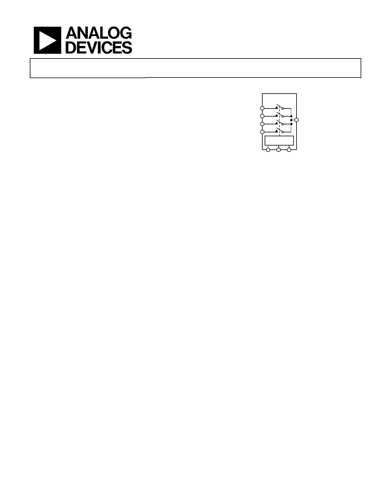
FUNCTIONAL BLOCK DIAGRAM
ADG5404
S1
S2
D
S3
S4
1 OF 4
DECODER
A0 A1 EN
Figure 1.
GENERAL DESCRIPTION
The ADG5404 is a complementary metal-oxide semiconductor
(CMOS) analog multiplexer, comprising four single channels.
The on-resistance profile is very flat over the full analog input
range, ensuring excellent linearity and low distortion when
switching audio signals.
The ADG5404 is designed on a trench process, which guards
against latch-up. A dielectric trench separates the P and N
channel transistors, thereby preventing latch-up even under
severe overvoltage conditions.
The ADG5404 switches one of four inputs to a common output,
D, as determined by the 3-bit binary address lines, A0, A1, and
EN. Logic 0 on the EN pin disables the device. Each switch
conducts equally well in both directions when on and has an
input signal range that extends to the supplies. In the off condi-
tion, signal levels up to the supplies are blocked. All switches
exhibit break-before-make switching action.
PRODUCT HIGHLIGHTS
1. Trench Isolation Guards Against Latch-Up. A dielectric
trench separates the P and N channel transistors, thereby
preventing latch-up even under severe overvoltage
conditions.
2. Low RON.
3. Dual-Supply Operation. For applications where the analog
signal is bipolar, the ADG5404 can be operated from dual
supplies of up to ±22 V.
4. Single-Supply Operation. For applications where the
analog signal is unipolar, the ADG5404 can be operated
from a single-rail power supply of up to 40 V.
5. 3 V logic-compatible digital inputs: VIH = 2.0 V, VIL = 0.8 V.
6. No VL logic power supply required.
Rev. 0
Information furnished by Analog Devices is believed to be accurate and reliable. However, no
responsibility is assumed by Analog Devices for its use, nor for any infringements of patents or other
rights of third parties that may result from its use. Specifications subject to change without notice. No
license is granted by implication or otherwise under any patent or patent rights of Analog Devices.
Trademarksandregisteredtrademarksarethepropertyoftheirrespectiveowners.
One Technology Way, P.O. Box 9106, Norwood, MA 02062-9106, U.S.A.
Tel: 781.329.4700
www.analog.com
Fax: 781.461.3113
©2010 Analog Devices, Inc. All rights reserved.
1 page 
DataSheet.in
ADG5404
+12 V SINGLE SUPPLY
VDD = 12 V ± 10%, VSS = 0 V, GND = 0 V, unless otherwise noted.
Table 3.
Parameter
ANALOG SWITCH
Analog Signal Range
On Resistance, RON
On-Resistance Match
Between Channels, ∆RON
On-Resistance Flatness, RFLAT(ON)
LEAKAGE CURRENTS
Source Off Leakage, IS (Off)
Drain Off Leakage, ID (Off)
Channel On Leakage, ID, IS (On)
DIGITAL INPUTS
Input High Voltage, VINH
Input Low Voltage, VINL
Input Current, IINL or IINH
25°C
19
22
0.4
0.8
4.4
5.5
±0.02
±0.25
±0.05
±0.4
±0.05
±0.4
0.002
Digital Input Capacitance, CIN
DYNAMIC CHARACTERISTICS1
Transition Time, tTRANSITION
tON (EN)
tOFF (EN)
Break-Before-Make Time Delay, tD
5
266
358
260
339
135
162
125
Charge Injection, QINJ
Off Isolation
Channel-to-Channel Crosstalk
Total Harmonic Distortion + Noise
92
−78
−58
0.075
−3 dB Bandwidth
Insertion Loss
CS (Off)
CD (Off)
CD, CS (On)
POWER REQUIREMENTS
IDD
VDD
43
−1.36
22
105
140
40
50
−40°C to +85°C −40°C to +125°C Unit
Test Conditions/Comments
27
1
6.5
±0.75
±2
±2
0 V to VDD
31
1.2
7.5
±3.5
±12
±12
V
Ω typ
Ω max
Ω typ
Ω max
Ω typ
Ω max
nA typ
nA max
nA typ
nA max
nA typ
nA max
VS = 0 V to 10 V, IS = −10 mA; see Figure 23
VDD = 10.8 V, VSS = 0 V
VS = 0 V to 10 V, IS = −10 mA
VS = 0 V to 10 V, IS = −10 mA
VDD = 13.2 V, VSS = 0 V
VS = 1 V/10 V, VD = 10 V/1 V; see Figure 24
VS = 1 V/10 V, VD = 10 V/1 V; see Figure 24
VS = VD = 1 V/10 V; see Figure 25
2.0 V min
0.8 V max
μA typ
VIN = VGND or VDD
±0.1 μA max
pF typ
446 515
423 485
189 210
45
65
9/40
ns typ
ns max
ns typ
ns max
ns typ
ns max
ns typ
ns min
pC typ
dB typ
dB typ
% typ
MHz typ
dB typ
pF typ
pF typ
pF typ
μA typ
μA max
V min/max
RL = 300 Ω, CL = 35 pF
VS = +8 V; see Figure 30
RL = 300 Ω, CL = 35 pF
VS = 8 V; see Figure 32
RL = 300 Ω, CL = 35 pF
VS = 8 V; see Figure 32
RL = 300 Ω, CL = 35 pF
VS1 = VS2 = 8 V; see Figure 31
VS = 6 V, RS = 0 Ω, CL = 1 nF; see Figure 33
RL = 50 Ω, CL = 5 pF, f = 1MHz; see Figure 26
RL = 50 Ω, CL = 5 pF, f = 1 MHz; see Figure 28
RL = 1k Ω, 6 V p-p, f = 20 Hz to 20 kHz;
see Figure 29
RL = 50 Ω, CL = 5 pF; see Figure 27
RL = 50 Ω, CL = 5 pF, f = 1 MHz; see Figure 27
VS = 6 V, f = 1 MHz
VS = 6 V, f = 1 MHz
VS = 6 V, f = 1 MHz
VDD = 13.2 V
Digital inputs = 0 V or VDD
GND = 0 V, VSS = 0 V
1 Guaranteed by design; not subject to production test.
Rev. 0 | Page 5 of 20
5 Page 
DataSheet.in
30
VDD = 12V
VSS = 0V
25
20
15
10
TA = +125°C
TA = +85°C
TA = +25°C
TA = –40°C
5
0
0 2 4 6 8 10 12
VS, VD (V)
Figure 10. RON as a Function of VD (VS) for Different Temperatures,
12 V Single Supply
16
14
12 TA = +125°C
10 TA = +85°C
8 TA = +25°C
6 TA = –40°C
4
2
VDD = 36V
VSS = 0V
0
0 5 10 15 20 25 30 35 40
VS, VD (V)
Figure 11. RON as a Function of VD (VS) for Different Temperatures,
36 V Single Supply
1.0
VDD = +15V
VSS = –15V
VBIAS = +10V/–10V
0.5
ID, IS (ON) + +
ID (OFF) – +
IS (OFF) + –
0
–0.5
–1.0
IS (OFF) – +
ID, IS (ON) – –
ID (OFF) + –
–1.5
0
25 50 75 100 125
TEMPERATURE (°C)
Figure 12. Leakage Currents vs. Temperature, ±15 V Dual Supply
ADG5404
1.0
VDD = +20V
VSS = –20V
VBIAS = +15V/–15V
0.5
0
ID, IS (ON) + +
ID (OFF) – +
IS (OFF) + –
–0.5 IS (OFF) – +
–1.0
ID, IS (ON) – –
ID (OFF) + –
–1.5
–2.0
0
25 50 75 100 125
TEMPERATURE (°C)
Figure 13. Leakage Currents vs. Temperature, ±20 V Dual Supply
0.6
VDD = 12V
VSS = 0V
VBIAS = 1V/10V
0.4
0.2
ID, IS (ON) + +
ID (OFF) – +
IS (OFF) + –
0
–0.2
–0.4
IS (OFF) – +
ID, IS (ON) – –
ID (OFF) + –
–0.6
0
25 50 75 100
TEMPERATURE (°C)
125
Figure 14. Leakage Currents vs. Temperature, 12 V Single Supply
1.0
VDD = 36V
VSS = 0V
VBIAS = 1V/30V
0.5
0
IS (OFF) + –
ID, IS (ON) + +
ID (OFF) – +
–0.5
–1.0
–1.5
IS (OFF) – +
ID, IS (ON) – –
ID (OFF) + –
–2.0
0 25 50 75 100 125
TEMPERATURE (°C)
Figure 15. Leakage Currents vs. Temperature, 36 V Single Supply
Rev. 0 | Page 11 of 20
11 Page | ||
| Páginas | Total 20 Páginas | |
| PDF Descargar | [ Datasheet ADG5404.PDF ] | |
Hoja de datos destacado
| Número de pieza | Descripción | Fabricantes |
| ADG5401 | Single SPST Switch | Analog Devices |
| ADG5404 | 4-Channel Multiplexer | Analog Devices |
| ADG5404F | 4-Channel Multiplexer | Analog Devices |
| ADG5408 | (ADG5408 / ADG5409) High Voltage Latch-Up Proof | Analog Devices |
| Número de pieza | Descripción | Fabricantes |
| SLA6805M | High Voltage 3 phase Motor Driver IC. |
Sanken |
| SDC1742 | 12- and 14-Bit Hybrid Synchro / Resolver-to-Digital Converters. |
Analog Devices |
|
DataSheet.es es una pagina web que funciona como un repositorio de manuales o hoja de datos de muchos de los productos más populares, |
| DataSheet.es | 2020 | Privacy Policy | Contacto | Buscar |