|
|
|
PDF 24AA64 Data sheet ( Hoja de datos )
| Número de pieza | 24AA64 | |
| Descripción | 64K I2C Serial EEPROM | |
| Fabricantes | Microchip Technology | |
| Logotipo | ||
Hay una vista previa y un enlace de descarga de 24AA64 (archivo pdf) en la parte inferior de esta página. Total 30 Páginas | ||
|
No Preview Available !
24AA64/24LC64/24FC64
64K I2C™ Serial EEPROM
Device Selection Table
Part
Number
VCC
Range
Max. Clock
Frequency
24AA64
24LC64
24FC64
Note 1:
2:
1.7-5.5
400 kHz(1)
2.5-5.5
1.7-5.5
400 kHz
1 MHz(2)
100 kHz for VCC <2.5V.
400 kHz for VCC <2.5V.
Temp.
Ranges
I, E
I, E
I
Features:
• Single-Supply with Operation down to 1.7V for
24AA64/24FC64 Devices, 2.5V for 24LC64
Devices
• Low-Power CMOS Technology:
- Active current 3 mA, max.
- Standby current 1 A, max.
• 2-Wire Serial Interface, I2C™ Compatible
• Packages with 3 Address Pins are Cascadable up
to 8 Devices
• Schmitt Trigger Inputs for Noise Suppression
• Output Slope Control to Eliminate Ground Bounce
• 100 kHz and 400 kHz Clock Compatibility
• 1 MHz Clock for FC versions
• Page Write Time 5 ms, max.
• Self-timed Erase/Write Cycle
• 32-Byte Page Write Buffer
• Hardware Write-Protect
• ESD Protection > 4,000V
• More than 1 Million Erase/Write Cycles
• Data Retention > 200 Years
• Factory Programming Available
• Packages include 8-lead PDIP, SOIC, SOIJ,
TSSOP, X-Rotated TSSOP, MSOP, DFN, TDFN,
5-lead SOT-23 or Chip Scale
• Pb-Free and RoHS Compliant
• Temperature Ranges:
- Industrial (I): -40°C to +85°C
- Automotive (E): -40°C to +125°C
Description:
The Microchip Technology Inc. 24AA64/24LC64/
24FC64 (24XX64*) is a 64 Kbit Electrically Erasable
PROM. The device is organized as a single block of
8K x 8-bit memory with a 2-wire serial interface. Low-
voltage design permits operation down to 1.7V, with
standby and active currents of only 1 A and 3 mA,
respectively. It has been developed for advanced, low-
power applications such as personal communications
or data acquisition. The 24XX64 also has a page write
capability for up to 32 bytes of data. Functional
address lines allow up to eight devices on the same
bus, for up to 512 Kbits address space. The 24XX64 is
available in the standard 8-pin PDIP, surface mount
SOIC, SOIJ, TSSOP, DFN, TDFN and MSOP
packages. The 24XX64 is also available in the 5-lead
SOT-23, and Chip Scale packages.
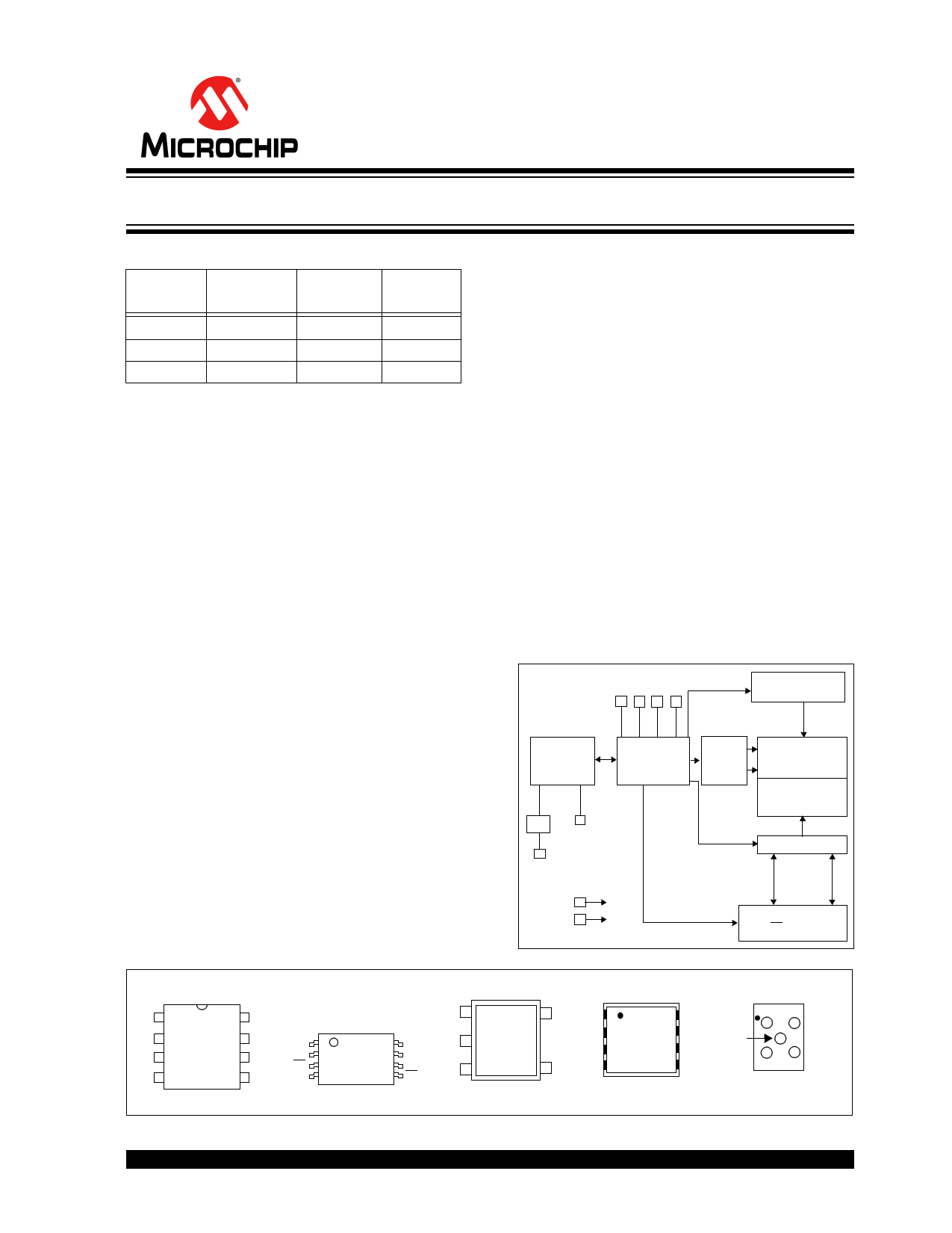
Block Diagram
A0 A1 A2 WP
HV
Generator
I/O
Control
Logic
I/O
SCL
SDA
VCC
VSS
Memory
Control
Logic
XDEC
EEPROM
Array
Page
Latches
YDEC
Sense Amp.
R/W Control
Package Types
PDIP/MSOP/SOIC/SOIJ/TSSOP
A0 1
8 VCC
X-Rotated TSSOP
(X/ST)
SCL
A1 2
A2 3
VSS 4
7 WP
WP 1
6
SCL
VCC
A0
2
3
5 SDA A1 4
8 SCL VSS
7 SDA
6
5
VSS
A2
SDA
Note 1: Available in I-temp, “AA” only.
SOT-23
15
2
34
DFN/TDFN
WP A0 1
A1 2
A2 3
VCC VSS 4
8 VCC
7 WP
6 SCL
5 SDA
CS (Chip Scale)(1)
VCC
WP
SCL
12
3
45
VSS
SDA
(Top Down View,
Balls Not Visible)
* 24XX64 is used in this document as a generic part number for the 24AA64/24LC64/24FC64 devices.
1997-2012 Microchip Technology Inc.
DS21189T-page 1
1 page 
24AA64/24LC64/24FC64
2.0 PIN DESCRIPTIONS
The descriptions of the pins are listed in Table 2-1.
TABLE 2-1: PIN FUNCTION TABLE
Name PDIP
SOIC
TSSOP
Rotated
TSSOP
DFN(1)
TDFN(1)
MSOP
SOT-23
CS
Description
A0 1
1
1
3
1 1 1 — — Chip Address Input
A1 2
2
2
4
2 2 2 — — Chip Address Input
A2 3
3
3
5
3 3 3 — — Chip Address Input
VSS
4
4
4
6
444
2 2 Ground
SDA 5
5
5
7
555
3 5 Serial Address/Data I/O
SCL 6
6
6
8
666
1 4 Serial Clock
WP 7
7
7
1
777
5 3 Write-Protect Input
VCC 8
8
8
2
888
4 1 +1.7V to 5.5V Power Supply
Note 1: The exposed pad on the DFN/TDFN packages can be connected to VSS or left floating.
2.1 A0, A1, A2 Chip Address Inputs
The A0, A1 and A2 inputs are used by the 24XX64 for
multiple device operation. The levels on these inputs
are compared with the corresponding bits in the slave
address. The chip is selected if the compare is true.
Up to eight devices may be connected to the same bus
by using different Chip Select bit combinations. These
inputs must be connected to either VCC or VSS.
In most applications, the chip address inputs A0, A1
and A2 are hard-wired to logic ‘0’ or logic ‘1’. For
applications in which these pins are controlled by a
microcontroller or other programmable device, the chip
address pins must be driven to logic ‘0’ or logic ‘1’
before normal device operation can proceed. Address
pins are not available in the SOT-23 or Chip Scale
packages.
2.2 Serial Data (SDA)
SDA is a bidirectional pin used to transfer addresses
and data into and out of the device. Since it is an open-
drain terminal, the SDA bus requires a pull-up resistor
to VCC (typical 10 k for 100 kHz, 2 kfor 400 kHz).
For normal data transfer, SDA is allowed to change
only during SCL low. Changes during SCL high are
reserved for indicating the Start and Stop conditions.
2.3 Serial Clock (SCL)
The SCL input is used to synchronize the data transfer
from and to the device.
2.4 Write-Protect (WP)
This pin must be connected to either VSS or VCC. If tied
to VSS, write operations are enabled. If tied to VCC,
write operations are inhibited but read operations are
not affected.
3.0 FUNCTIONAL DESCRIPTION
The 24XX64 supports a bidirectional, 2-wire bus and
data transmission protocol. A device that sends data
onto the bus is defined as transmitter, while a device
receiving data is defined as a receiver. The bus has to
be controlled by a master device which generates the
Serial Clock (SCL), controls the bus access and
generates the Start and Stop conditions, while the
24XX64 works as slave. Both master and slave can
operate as transmitter or receiver, but the master
device determines which mode is activated.
1997-2012 Microchip Technology Inc.
DS21189T-page 5
5 Page 
24AA64/24LC64/24FC64
8.0 READ OPERATION
Read operations are initiated in the same way as write
operations, with the exception that the R/W bit of the
control byte is set to one. There are three basic types
of read operations: current address read, random read
and sequential read.
8.1 Current Address Read
The 24XX64 contains an address counter that main-
tains the address of the last word accessed, internally
incremented by one. Therefore, if the previous read
access was to address ‘n’ (n is any legal address), the
next current address read operation would access data
from address n + 1.
Upon receipt of the control byte with R/W bit set to one,
the 24XX64 issues an acknowledge and transmits the
eight-bit data word. The master will not acknowledge
the transfer, but does generate a Stop condition and the
24XX64 discontinues transmission (Figure 8-1).
8.2 Random Read
Random read operations allow the master to access
any memory location in a random manner. To
perform this type of read operation, the word address
must first be set. This is accomplished by sending
the word address to the 24XX64 as part of a write
operation (R/W bit set to ‘0’). Once the word address
is sent, the master generates a Start condition
following the acknowledge.
FIGURE 8-1:
CURRENT ADDRESS READ
S
Bus Activity T Control
Master
A
R
Byte
T
SDA Line
S
Bus Activity
This terminates the write operation, but not before
the internal Address Pointer is set. The master then
issues the control byte again, but with the R/W bit set
to a one. The 24XX64 will then issue an acknowl-
edge and transmit the 8-bit data word. The master
will not acknowledge the transfer, but does generate
a Stop condition, which causes the 24XX64 to
discontinue transmission (Figure 8-2). After a
random Read command, the internal address coun-
ter will point to the address location following the one
that was just read.
8.3 Sequential Read
Sequential reads are initiated in the same way as
random reads, except that once the 24XX64 transmits
the first data byte, the master issues an acknowledge as
opposed to the Stop condition used in a random read.
This acknowledge directs the 24XX64 to transmit the
next sequentially-addressed 8-bit word (Figure 8-3).
Following the final byte being transmitted to the master,
the master will NOT generate an acknowledge, but will
generate a Stop condition. To provide sequential reads,
the 24XX64 contains an internal Address Pointer which
is incremented by one at the completion of each
operation. This Address Pointer allows the entire
memory contents to be serially read during one opera-
tion. The internal Address Pointer will automatically roll
over from address 1FFF to address 0000 if the master
acknowledges the byte received from the array address
1FFF.
Data (n)
A
C
K
S
T
O
P
P
N
O
A
C
K
1997-2012 Microchip Technology Inc.
DS21189T-page 11
11 Page | ||
| Páginas | Total 30 Páginas | |
| PDF Descargar | [ Datasheet 24AA64.PDF ] | |
Hoja de datos destacado
| Número de pieza | Descripción | Fabricantes |
| 24AA64 | 64K I2C Serial EEPROM | Microchip Technology |
| 24AA64F | EEPROM | Microchip |
| 24AA65 | 64K 1.8V I2C Smart Serial EEPROM | MicrochipTechnology |
| 24AA65-P | 64K 1.8V I2C Smart Serial EEPROM | MicrochipTechnology |
| Número de pieza | Descripción | Fabricantes |
| SLA6805M | High Voltage 3 phase Motor Driver IC. |
Sanken |
| SDC1742 | 12- and 14-Bit Hybrid Synchro / Resolver-to-Digital Converters. |
Analog Devices |
|
DataSheet.es es una pagina web que funciona como un repositorio de manuales o hoja de datos de muchos de los productos más populares, |
| DataSheet.es | 2020 | Privacy Policy | Contacto | Buscar |