|
|
|
PDF LTC3520 Data sheet ( Hoja de datos )
| Número de pieza | LTC3520 | |
| Descripción | Synchronous 1A Buck-Boost and 600mA Buck Converters | |
| Fabricantes | Linear Technology | |
| Logotipo | ||
Hay una vista previa y un enlace de descarga de LTC3520 (archivo pdf) en la parte inferior de esta página. Total 24 Páginas | ||
|
No Preview Available !
FEATURES
■ Dual High Efficiency DC/DC Converters:
Buck-Boost (VOUT: 2.2V to 5.25V, IOUT = 1A at
VOUT = 3.3V, VIN ≥ 3V)
Buck (VOUT: 0.8V to VIN, IOUT = 600mA)
■ 2.2V to 5.5V Input Voltage Range
■ Pin-Selectable Burst Mode® Operation
www■.DaUtnacShoememt4Uit.cteodmGain Block for LDO Controller,
Battery Good Indication or Sequencing
■ Programmable 100kHz to 2MHz Switching Frequency
■ 55µA Total Quiescent Current for Both Converters in
Burst Mode Operation
■ Thermal and Overcurrent Protection
■ <1µA Quiescent Current in Shutdown
■ 24-Lead 4mm × 4mm QFN Package
APPLICATIONS
■ Portable Media Players
■ Digital Cameras
■ Handheld PCs, PDAs
■ GPS Receivers
, LT, LTC, LTM and Burst Mode are registered trademarks of Linear Technology
Corporation. All other trademarks are the property of their respective owners. Protected by
U.S. Patents, including 5481178, 6166527, 6304066, 6404251, 6580258.
LTC3520
Synchronous 1A
Buck-Boost and 600mA
Buck Converters
DESCRIPTION
The LTC®3520 combines 1A buck-boost and 600mA
synchronous buck DC/DC converters in a tiny 4mm ×
4mm package. A programmable switching frequency
allows the efficiency to be optimized while minimizing
the solution footprint. Both converters feature soft-start
and current limit protection. The uncommitted gain block
can be configured as an LDO or utilized as a battery-good
comparator.
The buck converter is current mode controlled with internal
synchronous rectification to improve efficiency. Pin-select-
able Burst Mode operation can be enabled to improve light
load efficiency, or the buck converter can be operated in
low noise PWM mode for sensitive applications.
The buck-boost converter provides continuous conduc-
tion operation to maximize efficiency and minimize noise.
At light loads, use of Burst Mode operation will improve
efficiency.
The LTC3520 provides a <1µA shutdown mode and over-
temperature shutdown on both converters. The LTC3520
is available in a low profile (0.75mm) 24-lead 4mm ×
4mm QFN package.
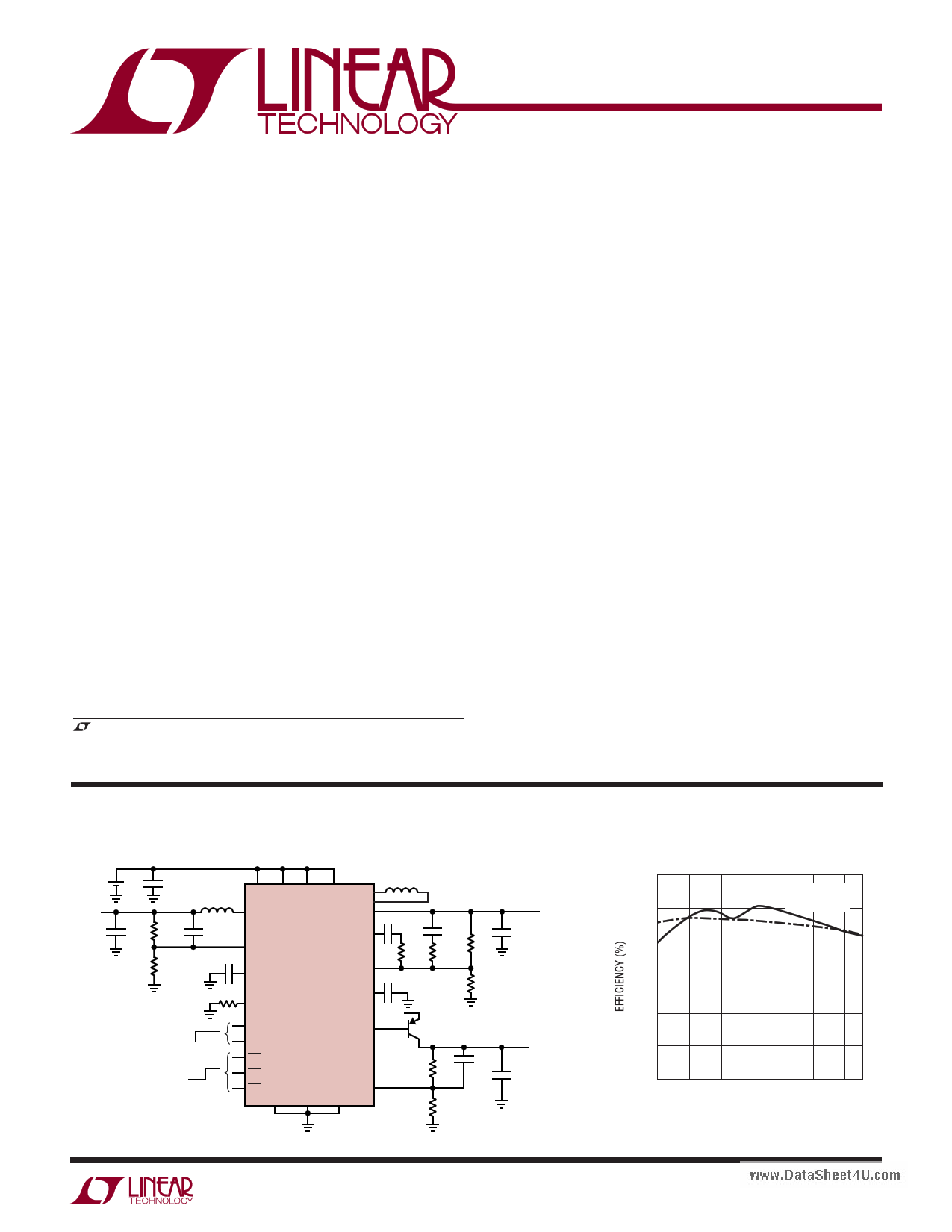
TYPICAL APPLICATION
3.3V at 500mA, 1.8V at 600mA and 1.5V at 200mA Converter
VIN
2.2V TO
5.5V
VOUT2
1.8V
600mA
10µF
22µF
255k
200k
BURST
4.7µH
PVIN1 PVIN2 PVIN3 SVIN SW1A
SW1B
SW2
VOUT1
4.7µH
470pF
27pF
FB2
0.01µF
SS2
54.9k
RT
LTC3520
VC1
15k
FB1
0.01µF
SS1
VOUT2
PWM
PWM1
PWM2
AOUT
SD3
OFF ON
SD2
SD1 AIN
PGND1 SGND PGND2
56pF
10k
1M
309k
100k
33pF
110k
47µF
VOUT1
3.3V
500mA
1A FOR
VIN ≥ 3V
VOUT
1.5V
200mA
4.7µF
3520 TA01
Efficiency vs VIN
100
BUCK-BOOST
95 IOUT = 150mA
BUCK
90 IOUT = 250mA
85
80
75
70
2.2 2.7 3.2 3.7 4.2 4.7 5.2
VIN (V)
3520f
1
1 page 
TYPICAL PERFORMANCE CHARACTERISTICS
LTC3520
Buck Efficiency
Lithium-Ion to 1.8V
100
Burst Mode
90 OPERATION
80
70
60
50
800
PWM MODE
700
600
VIN = 4.2V 500
VIN = 3V
400
40
30
www.DataSheet4U.com20 L = SUMIDA
10 CDRH3D16NP-4R7N
RBURST = 249k
0
1 10
Burst Mode
OPERATION
POWER LOSS
100
LOAD CURRENT (mA)
300
200
100
0
1000
3520 G03
LDO Load
Transient Response
LDO VOUT
100mV/DIV
LOAD
CURRENT
100mA/DIV
(20mA TO
210mA STEP)
VIN = 3.6V
VOUT = 1.5V
50µs/DIV
3520 G05
COUT = 4.7µF
LDO INPUT VOLTAGE = 1.8V
Switching Frequency vs RT
10000
1000
100
10
100
RT (k)
Buck-Boost Load
Transient Response
VOUT
VIN = 5V
200mV/DIV
VOUT
VIN = 2.2V
500mV/DIV
LOAD CURRENT
500mA/DIV
COUT = 47µF
L = 4.7µH
VIN = 3.3V
200µs/DIV
1000
3520 G04
3520 G06
Buck Load Transient
Response (PWM Mode)
BUCK VOUT
100mV/DIV
LOAD CURRENT
500mA/DIV
(50mA TO
500mA STEP)
VIN = 3.6V
VOUT = 1.8V
COUT = 10µF
100µs/DIV
3520 G07
Buck Load Transient
Response (Burst Mode Operation)
BUCK VOUT
100mV/DIV
LOAD CURRENT
200mA/DIV
(5mA TO
300mA STEP)
VIN = 3.6V
VOUT = 1.8V
100µs/DIV
COUT = 22µF
RBURST = 249k
3520 G08
3520f
5
5 Page 
LTC3520
OPERATION
The LTC3520 combines a synchronous buck DC/DC
converter and a four-switch buck-boost DC/DC converter
in a single 4mm x 4mm QFN package. The buck-boost
converter utilizes a proprietary switching algorithm which
allows its output voltage to be regulated above, below, or
equal to the input voltage. The buck converter provides a
high efficiency lower voltage output and supports 100%
duty cycle operation to extend battery life. In Burst Mode
operation, the total quiescent current for both converters
is reduced to 55µA (typical). Both converters operate
wwws.yDnactahSrhoeneotu4Us.lcyofmrom a common internal oscillator whose
frequency is programmed via an external resistor. In ad-
dition, the LTC3520 contains an uncommitted gain block
which can be configured as a comparator for low battery
detection or as a power-good indicator. Alternatively, the
gain block can be utilized in conjunction with an external
PNP to create an LDO, thereby allowing the LTC3520 to
generate a third low noise output voltage.
BUCK CONVERTER OPERATION
PWM Mode Operation
When the PWM2 pin is held high, the LTC3520 buck converter
uses a constant-frequency, current mode control architec-
ture. Both the main (P-channel MOSFET) and synchronous
rectifier (N-channel MOSFET) switches are internal. At
the start of each oscillator cycle, the P-channel switch is
turned on and remains on until the current waveform with
superimposed slope compensation ramp exceeds the error
amplifier output. At this point, the synchronous rectifier is
turned on and remains on until the inductor current falls to
zero or a new switching cycle is initiated. As a result, the
buck converter operates with discontinuous inductor cur-
rent at light loads which improves efficiency. At extremely
light loads, the minimum on-time of the main switch will
be reached and the buck converter will begin turning off for
multiple cycles in order to maintain regulation.
Burst Mode Operation
Burst Mode operation is enabled by either connecting
PWM2 to ground through a resistor, RBURST, or by shorting
PWM2 to ground. The buck converter will automatically
transition between PWM mode at high load current and
Burst Mode operation at light currents. Typical curves for
the Burst Mode entry threshold are provided in the Typical
Performance Characteristics section of this datasheet.
Under dropout and near dropout conditions, Burst Mode
operation will not be entered.
The value of RBURST controls the load current at which
Burst Mode operation will be entered. Larger resistor
values will cause Burst Mode operation to be entered at
lighter load currents. However, if the value of RBURST is
too large, then the buck converter will not enter Burst
Mode operation at any current, especially when operating
with VIN close to the buck output voltage. Conversely, if
RBURST is too small, the ripple in Burst Mode operation
may become objectionable, especially at high input volt-
ages. For most applications, choosing RBURST = 301k
represents a reasonable compromise.
The output voltage ripple in Burst Mode operation is de-
pendent upon the value of RBURST, the input voltage, the
output voltage, the inductor value and the output capaci-
tor. The Burst Mode operation output voltage ripple can
be reduced by increasing the size of the output capacitor,
increasing the value of the inductor or increasing the
value of RBURST.
Low Dropout Operation
As the input voltage decreases to a value approaching the
output regulation voltage, the duty cycle increases toward
the maximum on-time. Further reduction of the supply
voltage will force the power P-channel MOSFET switch
to remain on for more than one cycle until 100% duty
cycle operation is reached and the power switch remains
on continuously. In this dropout state, the output voltage
will be determined by the input voltage less the resistive
voltage drop across the main switch and series resistance
of the inductor.
Slope Compensation
Current mode control requires the use of slope compensa-
tion to prevent subharmonic oscillations in the inductor
current waveform at high duty cycle operation. This is ac-
complished internally on the LTC3520 through the addition
of a compensating ramp to the current sense signal. In
some current mode ICs, current limiting is performed by
clamping the error amplifier voltage to a fixed maximum.
3520f
11
11 Page | ||
| Páginas | Total 24 Páginas | |
| PDF Descargar | [ Datasheet LTC3520.PDF ] | |
Hoja de datos destacado
| Número de pieza | Descripción | Fabricantes |
| LTC3520 | Synchronous 1A Buck-Boost and 600mA Buck Converters | Linear Technology |
| LTC3521 | 1A Buck-Boost DC/DC And Dual 600mA Buck DC/DC Converters | Linear Technology |
| LTC3522 | Synchronous 400mA Buck-Boost and 200mA Buck Converters | Linear Technology |
| LTC3523 | Synchronous 600mA Step-Up And 400mA Step-Down DC/DC Converters | Linear Technology Corporation |
| Número de pieza | Descripción | Fabricantes |
| SLA6805M | High Voltage 3 phase Motor Driver IC. |
Sanken |
| SDC1742 | 12- and 14-Bit Hybrid Synchro / Resolver-to-Digital Converters. |
Analog Devices |
|
DataSheet.es es una pagina web que funciona como un repositorio de manuales o hoja de datos de muchos de los productos más populares, |
| DataSheet.es | 2020 | Privacy Policy | Contacto | Buscar |