|
|
|
PDF H6006 Data sheet ( Hoja de datos )
| Número de pieza | H6006 | |
| Descripción | Failsafe Watchdog | |
| Fabricantes | EM Microelectronic - MARIN SA | |
| Logotipo | ||
Hay una vista previa y un enlace de descarga de H6006 (archivo pdf) en la parte inferior de esta página. Total 8 Páginas | ||
|
No Preview Available !
R EM MICROELECTRONIC - MARIN SA
H6006www.DataSheet4U.com
Failsafe Watchdog
Description
The H6006 is a monolithic low power CMOS device
combining a programmable digital timer and a series of
voltage comparators on the same chip. The device is
specially convenient for Watch-Dog functions such as
microprocessor and supply voltage monitoring. The
watchdog part is designed to be used in all applications
where it is important that after the occurrence of a
malfunction the microprocessor system is stopped to avoid
further damage. The timeout warning signal ( TO ) can be
used to try to reactivate the system before halting it. The
voltage monitoring part provides double security by
combining both unregulated voltage and regulated voltage
monitoring simultaneously. The H6006 initializes the power-
on reset after VIN reached VSH and VDD raises above 3.5 V. If
VIN drops below VSL, the H6006 gives an advanced warning
signal for register saving and if the voltage drops further
below VRL, RES goes active. The H6006 functions at any
supply voltage down to 1.5 V and is therefore particularly
suited for start-up and shut-down control of microprocessor
systems
Typical Operating Configuration
Features
Failsafe watchdog function: timeout warning after 1st
timeout period, reset after 2nd timeout period, reset
remains active to avoid further failures
Standard timeout period and power-on reset time
(10 ms), externally programmable if required
VIN monitoring with 3 standard or programmable trigger
voltages for: power-on reset initialization, advanced
power-fail warning ( SAVE ), reset at power-down ( RES )
VDD monitoring: power-on reset initialization enabled
only if VDD ≥ 3.5 V
Internal voltage reference
Works down to 1.5 V supply voltage
Push-pull or Open drain outputs
Low current consumption
Available for normal and extended temperature range
SO8 package
Applications
Microprocessor and microcontroller systems
Point of sales equipment
Telecom products
Automotive subsystems
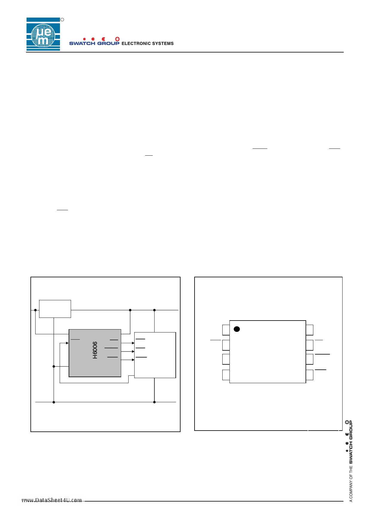
Pin Assignment
Voltage
Regulator
VIN
TCL
VSS
5V
VDD
TO
SAVE
RES
INT
NMI
RES
Micro-
processor
I/O
GND
Fig. 1
SO8
VIN
TCL
RC
VSS
H6006
VDD
TO
SAVE
RES
Fig. 2
Copyright © 2004, EM Microelectronic-Marin SA
1
www.emmicroelectronic.com
1 page 
R
H6006www.DataSheet4U.com
Pin Description
Pin Name Function
1 VIN Voltage monitoring input
2 TCL Timer clear input signal
3 RC RC oscillator tuning input
4 VSS GND terminal
5 RES Reset output
6 SAVE Save output
7 TO Timer output signal
8 VDD Positive supply voltage terminal
Functional Description
Table 6
Supply Lines
The circuit is powered through the VDD and VSS pins. It
monitors both its own VDD supply and a voltage applied to the
VIN input.
VDD Monitoring
During power-up the VIN monitoring is disabled and RES and
SAVE stay active low as long as VDD is below VON (3.5 V). As
soon as VDD reaches the VON level, the state of the outputs
depend on the watchdog timer and the volt-age at VIN relative
to the thresholds (see Fig. 3 and 4). If the supply voltage VDD
falls back below VOFF (1.5 V) the watchdog timer and the VIN
monitoring are disabled and the outputs SAVE and RES are
active low. The VDD line should be free of spikes.
VIN Monitoring
The analog voltage comparators compare the voltage applied
to VIN (typically connected to the input of the voltage regulator)
with the stabilized supply voltage VDD (versions B1, A2, B2) or
with the bandgap voltage (versions A3, B3) (see Fig. 7). At
power-up, when VDD reached VON and VIN reaches the VSH
level, the SAVE output goes high, and the timer starts
running, setting RES high after the time TTO (see Fig. 4). If VIN
falls below VSL, the SAVE output goes low and stays low until
VIN rises again above VSH. If VIN falls below the voltage VRL, the
RES output will go low and the on-chip timer will stop. When
VIN rises again above VSH, the timer will initiate a power-up
sequence. The RES output may however be influenced
independently of the voltage VIN by the timer action, see
section “Combined Voltage and Timer Action”. Monitoring the
rough DC side of the regulator as shown in Fig. 12 is the only
way to have advanced warning at power-down. Spikes on VIN
should be filtered if they are likely to drop below VSL.
The combination of VIN and VDD monitoring provide high
system security: if VIN rises much faster than VDD, then the
device starts the power-on sequence only when VDD reached
VON (Fig. 3). Short circuits on the regulated supply voltage can
be detected.
Voltage Thresholds on VIN
The H6006 is available with 3 different sets of thresholds:
Version B1: with internal voltage divider, resulting in
thresholds for direct monitoring of the unregulated voltage
without external components.
>9V
Voltage
Regulator
5V
VIN
VDD
SAVE
VSS RES
Note: The threshold levels are 9/8/7 V normally.These
are divided internally by 4 to give internal thres-
holds of 2.25 / 2 / 1.75 V. VDD = 5 V (thresholds
dependent on VDD). RVIN = ~ 100 kΩ.
Fig. 8
Version A2, B2: for monitoring of all unregulated voltage,
where custom programming is required. Fixed resistor
values can be used for programming.
any voltage
Voltage
Regulator
5V
VIN
VDD
SAVE
VSS RES
Note : the internal threshold levels are 2.25 / 2.00 / 1.75 V
at VDD = 5 V (thresholds dependent on VDD)
RVIN = ~ 100 MΩ.
Fig. 9
Version A3, B3: for monitoring of regulated voltage, where
no unregulated voltage is available (the tolerance is ±10 %,
see Table 4. For tighter tolerances, trimming can be used,
see Fig. 10).
5 V ± 10%
VIN VDD
SAVE
VSS RES
Note: the internal threshold levels are 2.00 / 1.95 / 1.90 V
(thresholds dependent on the internal bandgap
reference) RVIN = ~ 100 MΩ.
Fig. 10
Copyright © 2004, EM Microelectronic-Marin SA
5
www.emmicroelectronic.com
5 Page | ||
| Páginas | Total 8 Páginas | |
| PDF Descargar | [ Datasheet H6006.PDF ] | |
Hoja de datos destacado
| Número de pieza | Descripción | Fabricantes |
| H6006 | Failsafe Watchdog | EM Microelectronic - MARIN SA |
| Número de pieza | Descripción | Fabricantes |
| SLA6805M | High Voltage 3 phase Motor Driver IC. |
Sanken |
| SDC1742 | 12- and 14-Bit Hybrid Synchro / Resolver-to-Digital Converters. |
Analog Devices |
|
DataSheet.es es una pagina web que funciona como un repositorio de manuales o hoja de datos de muchos de los productos más populares, |
| DataSheet.es | 2020 | Privacy Policy | Contacto | Buscar |