|
|
|
PDF IRF6638TRPbF Data sheet ( Hoja de datos )
| Número de pieza | IRF6638TRPbF | |
| Descripción | DirectFET Power MOSFET | |
| Fabricantes | International Rectifier | |
| Logotipo | ||
Hay una vista previa y un enlace de descarga de IRF6638TRPbF (archivo pdf) en la parte inferior de esta página. Total 10 Páginas | ||
|
No Preview Available !
PD - 97239
IRF6638PbF
IRF6638TRPbFwww.DataSheet4U.com
l RoHs Compliant
l Lead-Free (Qualified up to 260°C Reflow)
l Application Specific MOSFETs
l Ideal for CPU Core DC-DC Converters
l Low Conduction Losses
l High Cdv/dt Immunity
l Low Profile (<0.7mm)
l Dual Sided Cooling Compatible
l Compatible with existing Surface Mount Techniques
DirectFET Power MOSFET
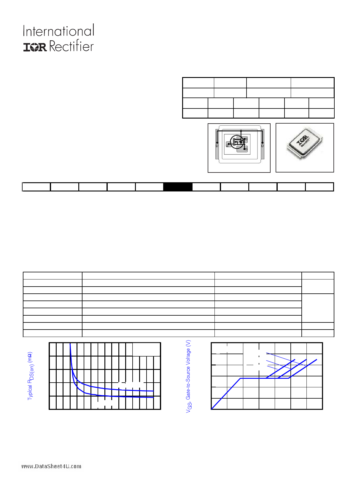
Typical values (unless otherwise specified)
VDSS
VGS
RDS(on)
RDS(on)
30V max ±20V max 2.2mΩ@ 10V 3.0mΩ@ 4.5V
Qg tot Qgd Qgs2 Qrr Qoss Vgs(th)
30nC 11nC 3.2nC 27nC 18.4nC 1.8V
MX
DirectFET ISOMETRIC
Applicable DirectFET Outline and Substrate Outline (see p.7,8 for details)
SQ SX ST
MQ MX MT MP
Description
The IRF6638PbF combines the latest HEXFET® Power MOSFET Silicon technology with the advanced DirectFETTM packaging to achieve
the lowest on-state resistance in a package that has the footprint of a SO-8 and only 0.6 mm profile. The DirectFET package is compatible
with existing layout geometries used in power applications, PCB assembly equipment and vapor phase, infra-red or convection soldering
techniques, when application note AN-1035 is followed regarding the manufacturing methods and processes. The DirectFET package allows
dual sided cooling to maximize thermal transfer in power systems, improving previous best thermal resistance by 80%.
The IRF6638PbF balances both low resistance and low charge along with ultra low package inductance to reduce both conduction and
switching losses. The reduced total losses make this product ideal for high efficiency DC-DC converters that power the latest generation of
processors operating at higher frequencies. The IRF6638PbF has been optimized for parameters that are critical in synchronous buck
including Rds(on), gate charge and Cdv/dt-induced turn on immunity. The IRF6638PbF offers particularly low Rds(on) and high Cdv/dt
immunity for synchronous FET applications.
Absolute Maximum Ratings
Parameter
Max.
Units
VDS Drain-to-Source Voltage
30 V
VGS
ID @ TA = 25°C
ID @ TA = 70°C
ID @ TC = 25°C
IDM
EAS
IAR
Gate-to-Source Voltage
eContinuous Drain Current, VGS @ 10V
eContinuous Drain Current, VGS @ 10V
fContinuous Drain Current, VGS @ 10V
gPulsed Drain Current
hSingle Pulse Avalanche Energy
ÃgAvalanche Current
±20
25
20 A
140
200
37 mJ
20 A
10 6.0
8
ID = 25A
5.0 ID= 20A
VDS= 24V
6
4.0
VDS= 15V
VDS= 6.0V
3.0
4
TJ = 125°C
2.0
2
0 TJ = 25°C
0 1 2 3 4 5 6 7 8 9 10 11 12 13 14 15 16
1.0
0.0
0
5 10 15 20 25 30 35
VGS, Gate -to -Source Voltage (V)
Notes:
Fig 1. Typical On-Resistance Vs. Gate Voltage
Click on this section to link to the appropriate technical paper.
Click on this section to link to the DirectFET Website.
Surface mounted on 1 in. square Cu board, steady state.
www.irf.com
QG Total Gate Charge (nC)
Fig 2. Typical Total Gate Charge vs Gate-to-Source Voltage
TC measured with thermocouple mounted to top (Drain) of part.
Repetitive rating; pulse width limited by max. junction temperature.
Starting TJ = 25°C, L = 0.19mH, RG = 25Ω, IAS = 20A.
1
07/13/06
1 page 
1000
100 TJ = 150°C
TJ = 25°C
TJ = -40°C
10
1
VGS = 0V
0
0.1 0.2 0.3 0.4 0.5 0.6 0.7 0.8 0.9 1.0 1.1
VSD, Source-to-Drain Voltage (V)
Fig 10. Typical Source-Drain Diode Forward Voltage
150
IRF6638PbF
1000
www.DataSheet4U.com
OPERATION IN THIS AREA
LIMITED BY RDS(on)
100
100µsec
1msec
10
10msec
1
Tc = 25°C
Tj = 150°C
Single Pulse
0.1
01
10 100
VDS, Drain-to-Source Voltage (V)
Fig11. Maximum Safe Operating Area
2.5
125
100 2.0
75
ID = 250µA
50 1.5
25
0
25 50 75 100 125 150
TC , Case Temperature (°C)
Fig 12. Maximum Drain Current vs. Case Temperature
150
125
100
1.0
-75 -50 -25 0 25 50 75 100 125 150
TJ , Temperature ( °C )
Fig 13. Typical Threshold Voltage vs. Junction
Temperature
ID
TOP 5.5A
6.5A
BOTTOM 20A
75
50
25
www.irf.com
0
25 50 75 100 125 150
Starting TJ , Junction Temperature (°C)
Fig 14. Maximum Avalanche Energy Vs. Drain Current
5
5 Page | ||
| Páginas | Total 10 Páginas | |
| PDF Descargar | [ Datasheet IRF6638TRPbF.PDF ] | |
Hoja de datos destacado
| Número de pieza | Descripción | Fabricantes |
| IRF6638TRPbF | DirectFET Power MOSFET | International Rectifier |
| IRF6638TRPbF | DirectFET Power MOSFET | International Rectifier |
| Número de pieza | Descripción | Fabricantes |
| SLA6805M | High Voltage 3 phase Motor Driver IC. |
Sanken |
| SDC1742 | 12- and 14-Bit Hybrid Synchro / Resolver-to-Digital Converters. |
Analog Devices |
|
DataSheet.es es una pagina web que funciona como un repositorio de manuales o hoja de datos de muchos de los productos más populares, |
| DataSheet.es | 2020 | Privacy Policy | Contacto | Buscar |