|
|
|
PDF LC75853NW Data sheet ( Hoja de datos )
| Número de pieza | LC75853NW | |
| Descripción | 1/3 Duty LCD Display Drivers with Key Input Function | |
| Fabricantes | Sanyo Semicon Device | |
| Logotipo | ||
Hay una vista previa y un enlace de descarga de LC75853NW (archivo pdf) en la parte inferior de esta página. Total 24 Páginas | ||
|
No Preview Available !
Ordering number : ENN4967C
CMOS IC
LC75853NE, 75853NW
1/3 Duty LCD Display Drivers
with Key Input Function
Overview
The LC75853NE and LC75853NW are 1/3 duty LCD
display drivers that can directly drive up to 126 segments
and can control up to four general-purpose output ports.
These products also incorporate a key scan circuit that
accepts input from up to 30 keys to reduce printed circuit
board wiring.
Features
• Key input function for up to 30 keys (A key scan is
performed only when a key is pressed.)
• 1/3 duty - 1/2 bias and 1/3 duty - 1/3 bias drive schemes
can be controlled from serial data (up to 126 segments).
• Sleep mode and all segments off functions that are
controlled from serial data
• Segment output port/general-purpose output port
function switching that is controlled from serial data
• Serial data I/O supports CCB format communication
with the system controller.
• Direct display of display data without the use of a
decoder provides high generality.
• Provision of an on-chip voltage-detection type reset
circuit prevents incorrect displays.
• RC oscillator circuit
• CCB is a trademark of SANYO ELECTRIC CO., LTD.
• CCB is SANYO’s original bus format and all the bus
addresses are controlled by SANYO.
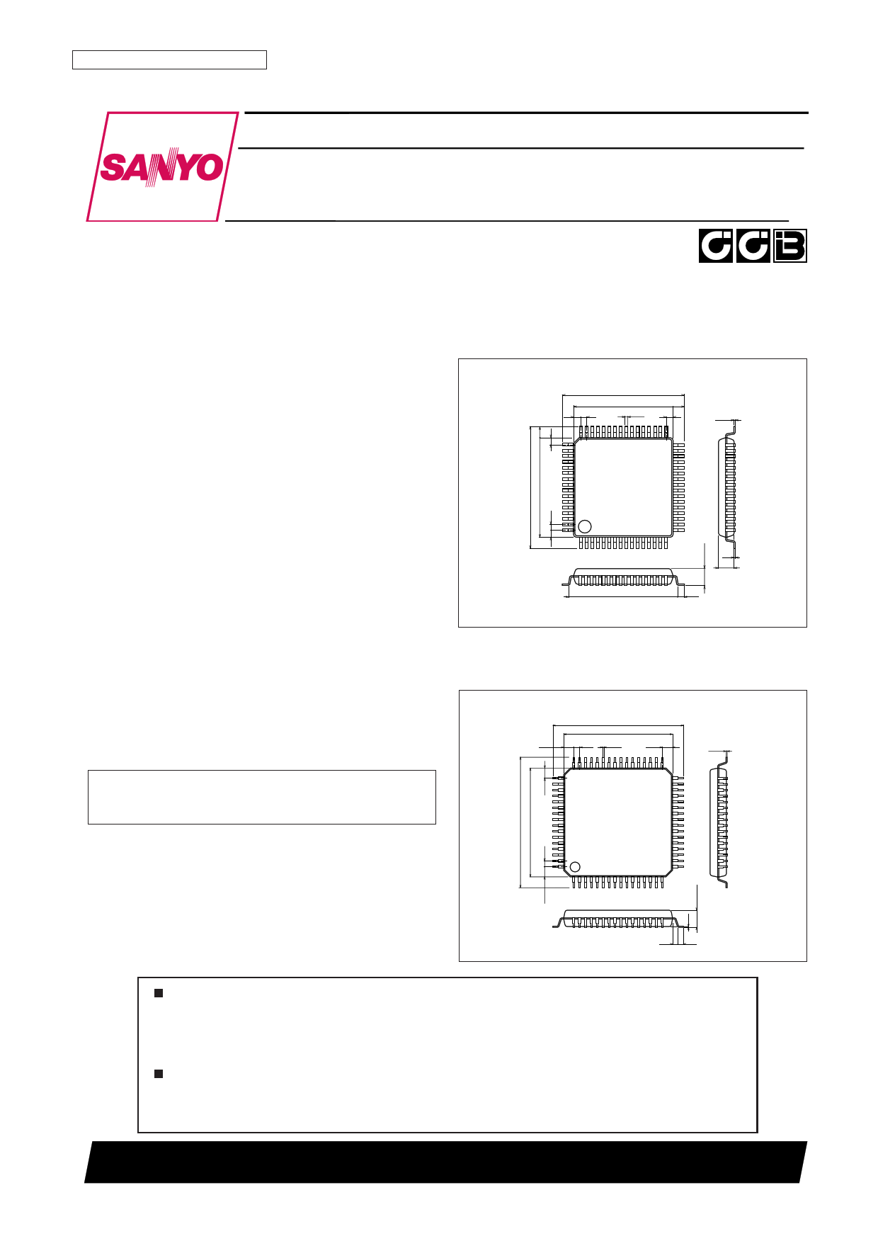
Package Dimensions
unit: mm
3159-QFP64E
1.0
48
49
[LC75853NE]
17.2
14.0 1.6
0.8 0.35 1.0
33
32
0.15
64
1
unit: mm
3190-SQFP64
17
16
0.1
2.7
15.6 0.8
SANYO: QFP64E
1.25
48
49
[LC75853NW]
12.0
10.0
0.5 0.18
1.25
33
32
0.15
64
1
17
16
0.5 0.5
SANYO: SQFP64
Any and all SANYO products described or contained herein do not have specifications that can handle
applications that require extremely high levels of reliability, such as life-support systems, aircraft’s
control systems, or other applications whose failure can be reasonably expected to result in serious
physical and/or material damage. Consult with your SANYO representative nearest you before using
any SANYO products described or contained herein in such applications.
SANYO assumes no responsibility for equipment failures that result from using products at values that
exceed, even momentarily, rated values (such as maximum ratings, operating condition ranges, or other
parameters) listed in products specifications of any and all SANYO products described or contained
herein.
SANYO Electric Co.,Ltd. Semiconductor Company
TOKYO OFFICE Tokyo Bldg., 1-10, 1 Chome, Ueno, Taito-ku, TOKYO, 110-8534 JAPAN
O3099TH (OT)/23099HA (OT)/N3095HA (OT)/52295TH (OT) No. 4967-1/24
1 page 
Block Diagram
LC75853NE, 75853NW
Pin Assignment
No. 4967-5/24
5 Page 
LC75853NE, 75853NW
Sleep Mode Functions
Sleep mode is set up by setting S0 or S1 in the control data to 1. The segment outputs will all go low and the common
outputs will also go low, and the oscillator on the OSC pin will stop (it will be started by a key press). This reduces
power dissipation. This mode is cleared by sending control data with both S0 and S1 set to 0. However, note that the
S1/P1 to S4/P4 outputs can be used as general-purpose output ports according to the state of the P0 and P1 control data
bits, even in sleep mode. (See the control data description for details.)
Key Scan Operation Functions
1. Key scan timing
The key scan period is 288 T (s). To reliably determine the on/off state of the keys, the LC75853NE/NW scans the
keys twice and determines that a key has been pressed when the key data agrees. It outputs a key data read request (a
low level on DO) 615 T (s) after starting a key scan. If the key data does not agree and a key was pressed at that
point, it scans the keys again. Thus the LC75853NE/NW cannot detect a key press shorter than 615 T (s).
Note: *3. In sleep mode the high/low state of these pins is determined by the S0 and S1 bits in the control data. Key scan output signals are not output
from pins that are set low.
2. In normal mode
• The pins KS1 to KS6 are set high
• When a key is pressed a key scan is started and the keys are scanned until all keys are released. Multiple key
presses are recognized by determining whether multiple key data bits are set.
• If a key is pressed for longer than 615 T (s) (where T = 1 ) the LC75853NE/NW outputs a key data read
fOSC
request (a low level on DO) to the controller. The controller acknowledges this request and reads the key data.
However, if CE is high during a serial data transfer, DO will be set high.
• After the controller reads the key data, the key data read request is cleared (DO is set high) and the
LC75853NE/NW performs another key scan. Also note that DO, being an open-drain output, requires a pull-up
resistor (between 1 and 10 kΩ).
No. 4967-11/24
11 Page | ||
| Páginas | Total 24 Páginas | |
| PDF Descargar | [ Datasheet LC75853NW.PDF ] | |
Hoja de datos destacado
| Número de pieza | Descripción | Fabricantes |
| LC75853NE | 1/3 Duty LCD Display Drivers with Key Input Function | Sanyo Semicon Device |
| LC75853NW | 1/3 Duty LCD Display Drivers with Key Input Function | Sanyo Semicon Device |
| Número de pieza | Descripción | Fabricantes |
| SLA6805M | High Voltage 3 phase Motor Driver IC. |
Sanken |
| SDC1742 | 12- and 14-Bit Hybrid Synchro / Resolver-to-Digital Converters. |
Analog Devices |
|
DataSheet.es es una pagina web que funciona como un repositorio de manuales o hoja de datos de muchos de los productos más populares, |
| DataSheet.es | 2020 | Privacy Policy | Contacto | Buscar |