|
|
|
PDF ISL95811 Data sheet ( Hoja de datos )
| Número de pieza | ISL95811 | |
| Descripción | Single Digitally Controlled Potentiometer | |
| Fabricantes | Intersil Corporation | |
| Logotipo | ||
Hay una vista previa y un enlace de descarga de ISL95811 (archivo pdf) en la parte inferior de esta página. Total 14 Páginas | ||
|
No Preview Available !
ISL95811
®
Single Digitally Controlled Potentiometer (XDCP™)
Data Sheet
October 6, 2008
FN6759.1
I2C Bus, 256 Taps, 5 Bytes General
Purpose Memory, Low Noise, Low Power
The ISL95811 integrates a digitally controlled potentiometer
(XDCP) and non-volatile memory on a monolithic CMOS
integrated circuit.
The digitally controlled potentiometer is implemented with a
combination of resistor elements and CMOS switches. The
position of the wiper is controlled by the user through the I2C
bus interface. The potentiometer has an associated volatile
Wiper Register (WR) and a non-volatile Initial Value Register
(IVR), that can be directly written to and read by the user.
The content of the WR controls the position of the wiper. At
power-up the device recalls the contents of the DCP’s IVR to
the WR.
The DCP can be used as three-terminal potentiometer or as
two-terminal variable resistor in a wide variety of applications
including control, parameter adjustments and signal
processing.
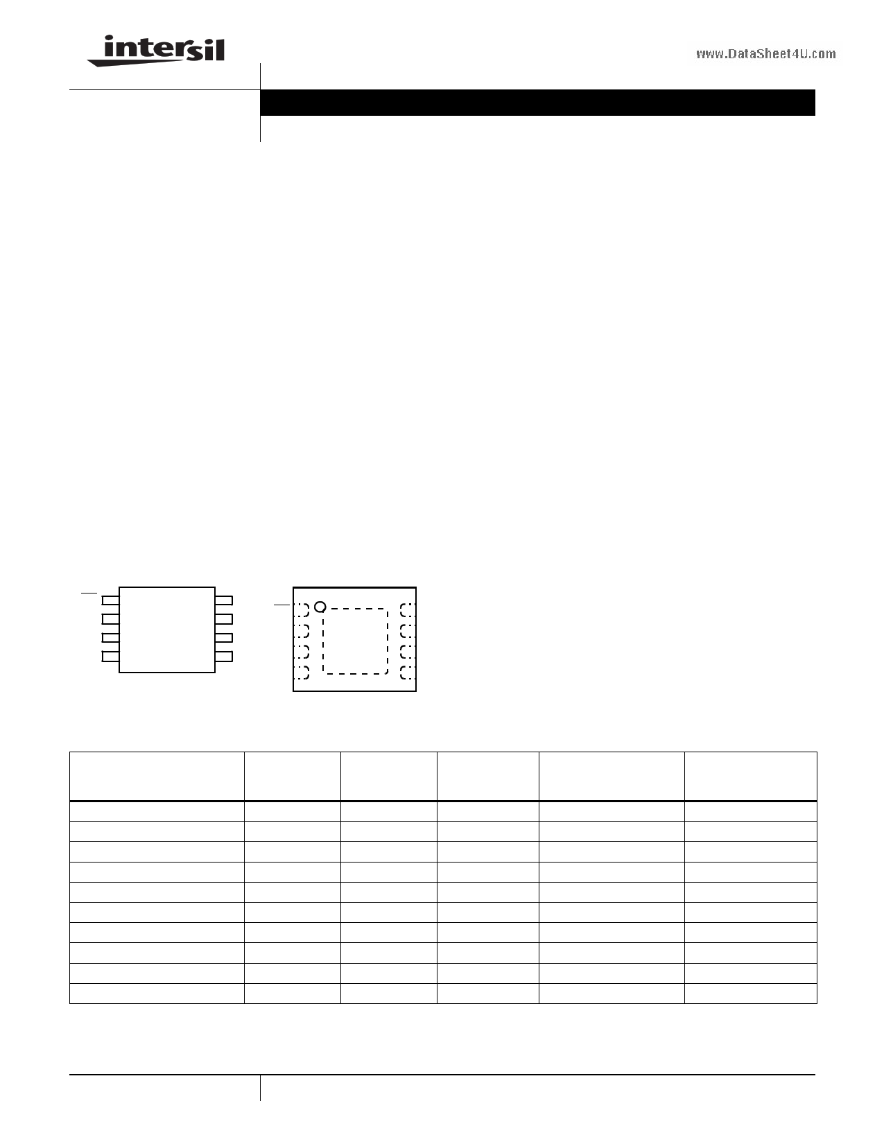
Pinouts
ISL95811
(8 LD MSOP)
TOP VIEW
ISL95811
(8 LD TDFN)
TOP VIEW
WP
SCL
SDA
GND
1
2
3
4
www.DataSheet4U.com
8 VCC
7
WP 1
RH
6 RL SCL 2
5 RW SDA 3
GND 4
8 VCC
7 RH
6 RL
5 RW
Features
• 256 Resistor Taps - 0.4% Resolution
• I2C Serial Interface
• 5 General Purpose Non-Volatile Bytes
• Non-volatile Storage of Wiper Position
• Write Protection
• Wiper Resistance: 70Ω Typical @ VCC = 3.3V
• Standby Current 10µA Max
• Power Supply: 2.7V to 5.5V
• 50kΩ, 10kΩ Total Resistance
• High Reliability
- Endurance: 1,000,000 Data Changes per Bit per
Register
- Register Data Retention: 50 Years @ T ≤ +55°C
• 8 Ld MSOP and 8 Ld TDFN Packaging
• Pb-Free (RoHS compliant)
Ordering Information
PART NUMBER
(Note)
PART
MARKING
RTOTAL
(kΩ)
TEMP.
RANGE
(°C)
PACKAGE
(Pb-Free)
PKG.
DWG. #
ISL95811WFUZ
5811W
10 -40 to +125 8 Ld MSOP
MDP0043
ISL95811WFUZ-T*
5811W
10 -40 to +125 8 Ld MSOP
MDP0043
ISL95811WFUZ-TK*
5811W
10 -40 to +125 8 Ld MSOP
MDP0043
ISL95811WFRTZ
811W
10 -40 to +125 8 Ld 3x3 TDFN
L8.3x3A
ISL95811WFRTZ-TK*
811W
10 -40 to +125 8 Ld 3x3 TDFN
L8.3x3A
ISL95811UFUZ
5811U
50 -40 to +125 8 Ld MSOP
MDP0043
ISL95811UFUZ-T*
5811U
50 -40 to +125 8 Ld MSOP
MDP0043
ISL95811UFUZ-TK*
5811U
50 -40 to +125 8 Ld MSOP
MDP0043
ISL95811UFRTZ
811U
50 -40 to +125 8 Ld 3x3 TDFN
L8.3x3A
ISL95811UFRTZ-TK*
811U
50 -40 to +125 8 Ld 3x3 TDFN
L8.3x3A
*Please refer to TB347 for details on reel specifications
NOTE: These Intersil Pb-free plastic packaged products employ special Pb-free material sets, molding compounds/die attach materials, and 100%
matte tin plate plus anneal (e3 termination finish, which is RoHS compliant and compatible with both SnPb and Pb-free soldering operations). Intersil
Pb-free products are MSL classified at Pb-free peak reflow temperatures that meet or exceed the Pb-free requirements of IPC/JEDEC J STD-020.
1 CAUTION: These devices are sensitive to electrostatic discharge; follow proper IC Handling Procedures.
1-888-INTERSIL or 1-888-468-3774 | Intersil (and design) is a registered trademark of Intersil Americas Inc.
XDCP is a trademark of Intersil Corporation. Copyright Intersil Americas Inc. 2008. All Rights Reserved
All other trademarks mentioned are the property of their respective owners.
1 page 
ISL95811
Operating Specifications Over the recommended operating conditions unless otherwise specified. (Continued)
SYMBOL
PARAMETER
TEST CONDITIONS
MIN TYP MAX
(Note 18) (Note 4) (Note 18) UNITS
fSCL
tIN
SCL Frequency
Pulse Width Suppression Time at
SDA and SCL Inputs
Any pulse narrower than the max spec is
suppressed.
400 kHz
50 ns
tAA
tBUF
SCL Falling Edge to SDA Output
Data Valid
Time the Bus Must be Free Before
the Start of a New Transmission
SCL falling edge crossing 30% of VCC, until
SDA exits the 30% to 70% of VCC window.
SDA crossing 70% of VCC during a STOP
condition, to SDA crossing 70% of VCC during
the following START condition.
1300
900 ns
ns
tLOW
tHIGH
tSU:STA
tHD:STA
tSU:DAT
tHD:DAT
tSU:STO
tHD:STO
tHD:STO:NV
tDH
Clock LOW Time
Measured at the 30% of VCC crossing.
Clock HIGH Time
Measured at the 70% of VCC crossing.
START Condition Setup Time
SCL rising edge to SDA falling edge. Both
crossing 70% of VCC.
START Condition Hold Time
From SDA falling edge crossing 30% of VCC to
SCL falling edge crossing 70% of VCC.
Input Data Setup Time
From SDA exiting the 30% to 70% of VCC
window, to SCL rising edge crossing 30% of
VCC
Input Data Hold Time
From SCL rising edge crossing 70% of VCC to
SDA entering the 30% to 70% of VCC window.
STOP Condition Setup Time
From SCL rising edge crossing 70% of VCC, to
SDA rising edge crossing 30% of VCC.
STOP Condition Hold Time for Read, From SDA rising edge to SCL falling edge. Both
or Volatile Only Write
crossing 70% of VCC.
STOP Condition Hold Time for Non- From SDA rising edge to SCL falling edge. Both
Volatile Write
crossing 70% of VCC.
Output Data Hold Time
From SCL falling edge crossing 30% of VCC,
until SDA enters the 30% to 70% of VCC
window.
1300
600
600
600
100
0
600
600
2
0
ns
ns
ns
ns
ns
ns
ns
ns
µs
ns
tR (Note 16) SDA and SCL Rise Time
www.DataSheet4U.com
From 30% to 70% of VCC
20 +
0.1 * Cb
250 ns
tF (Note 16) SDA and SCL Fall Time
From 70% to 30% of VCC
20 +
0.1 * Cb
250 ns
Cb (Note 16) Capacitive Loading of SDA or SCL Total on-chip and off-chip
10 400 pF
Rpu (Note 16)
SDA and SCL Bus Pull-Up Resistor Maximum is determined by tR and tF.
Off-Chip
For Cb = 400pF, max is about 2kΩ~2.5kΩ.
For Cb = 40pF, max is about 15kΩ~20kΩ
1
kΩ
tWC (Note 17) Non-Volatile Write Cycle Time
12 20 ms
tSU:WP
WP Setup Time
Before START condition
600 ns
tHD:WP
WP Hold Time
After STOP condition
600 ns
NOTES:
4. Typical values are for TA = +25°C and 3.3V supply voltage.
5. LSB: [V(RW)255 – V(RW)0]/255. V(RW)255 and V(RW)0 are V(RW) for the DCP register set to FF hex and 00 hex respectively. LSB is the
incremental voltage when changing from one tap to an adjacent tap.
6. ZS error = V(RW)0/LSB.
7. FS error = [V(RW)255 – VCC]/LSB.
8. DNL = [V(RW)i – V(RW)i-1]/LSB-1, for i = 1 to 255. i is the DCP register setting.
5 FN6759.1
October 6, 2008
5 Page 
ISL95811
Protocol Conventions
Data states on the SDA line can change only during SCL
LOW periods. SDA state changes during SCL HIGH are
reserved for indicating START and STOP conditions (see
Figure 17). On power-up of the ISL95811, the SDA pin is in
the input mode.
All I2C interface operations must begin with a START
condition, which is a HIGH to LOW transition of SDA while
SCL is HIGH. The ISL95811 continuously monitors the SDA
and SCL lines for the START condition and does not
respond to any command until this condition is met (see
Figure 17). A START condition is ignored during the
power-up sequence and during internal non-volatile write
cycles.
All I2C interface operations must be terminated by a STOP
condition, which is a LOW to HIGH transition of SDA while
SCL is HIGH (see Figure 17). A STOP condition at the end
of a read operation, or at the end of a write operation to
volatile bytes only places the device in its standby mode. A
STOP condition during a write operation to a non-volatile
byte initiates an internal non-volatile write cycle. The device
enters its standby state when the internal non-volatile write
cycle is completed.
An ACK, Acknowledge, is a software convention used to
indicate a successful data transfer. The transmitting device,
either master or slave, releases the SDA bus after
transmitting 8 bits. During the ninth clock cycle, the receiver
pulls the SDA line LOW to acknowledge the reception of the
8 bits of data (see Figure 18).
The ISL95811 responds with an ACK after recognition of a
START condition followed by a valid Identification Byte, and
once again after successful receipt of an Address Byte. The
ISL95811 also responds with an ACK after receiving a Data
Byte of a write operation. The master must respond with an
ACK after receiving a Data Byte of a read operation.
A valid Identification Byte contains 0101000 as the seven
MSBs. The LSB is the Read/Write bit. Its value is “1” for a
Read operation and “0” for a Write operation (see Table 4).
TABLE 4. IDENTIFICATION BYTE FORMAT
0 1 0 1 0 0 0 R/W
(MSB)
(LSB)
SCL
SDA
www.DataSheet4U.com
START
DATA
DATA
DATA
STABLE CHANGE STABLE
STOP
FIGURE 17. VALID DATA CHANGES, START, AND STOP CONDITIONS
SCL FROM
MASTER
SDA OUTPUT FROM
TRANSMITTER
1
89
HIGH IMPEDANCE
SDA OUTPUT FROM
RECEIVER
HIGH IMPEDANCE
START
FIGURE 18. ACKNOWLEDGE RESPONSE FROM RECEIVER
ACK
11 FN6759.1
October 6, 2008
11 Page | ||
| Páginas | Total 14 Páginas | |
| PDF Descargar | [ Datasheet ISL95811.PDF ] | |
Hoja de datos destacado
| Número de pieza | Descripción | Fabricantes |
| ISL95810 | Single Digitally Controlled Potentiometer | Intersil Corporation |
| ISL95811 | Single Digitally Controlled Potentiometer | Intersil Corporation |
| ISL95813 | Single Phase Core Controller | Intersil |
| Número de pieza | Descripción | Fabricantes |
| SLA6805M | High Voltage 3 phase Motor Driver IC. |
Sanken |
| SDC1742 | 12- and 14-Bit Hybrid Synchro / Resolver-to-Digital Converters. |
Analog Devices |
|
DataSheet.es es una pagina web que funciona como un repositorio de manuales o hoja de datos de muchos de los productos más populares, |
| DataSheet.es | 2020 | Privacy Policy | Contacto | Buscar |