|
|
|
PDF 513CS Data sheet ( Hoja de datos )
| Número de pieza | 513CS | |
| Descripción | MAX513 | |
| Fabricantes | Maxim Integrated Products | |
| Logotipo | ||
Hay una vista previa y un enlace de descarga de 513CS (archivo pdf) en la parte inferior de esta página. Total 16 Páginas | ||
|
No Preview Available !
19-0252; Rev 2; 5/96
Low-Cost, Triple, 8-Bit Voltage-Output DACs
with Serial Interface
_______________General Description
The MAX512/MAX513 contain three 8-bit, voltage-output
digital-to-analog converters (DAC A, DAC B, and DAC C).
Output buffer amplifiers for DACs A and B provide voltage
outputs while reducing external component count. The
output buffer for DAC A can source or sink 5mA to within
0.5V of VDD or VSS. The buffer for DAC B can source or
sink 0.5mA to within 0.5V of VDD or VSS. DAC C is
unbuffered, providing a third voltage output with increased
accuracy. The MAX512 operates with a single
+5V ±10% supply, and the MAX513 operates with a
+2.7V to +3.6V supply. Both devices can also operate
with split supplies.
The 3-wire serial interface has a maximum operating fre-
quency of 5MHz and is compatible with SPI™, QSPI™,
and Microwire™. The serial input shift register is 16 bits
long and consists of 8 bits of DAC input data and 8 bits
for DAC selection and shutdown. DAC registers can be
loofaC–d—Se–.d
independently or in parallel at the positive
A latched logic output is also available for
edge
auxil-
iary control.
Ultra-low power consumption and small packages
(14-pin DIP/SO) make the MAX512/MAX513 ideal for
portable and battery-powered applications. Supply cur-
rent is only 1mA, dropping to less than 1µA in shutdown.
Any of the three DACs can be independently shut down.
In shutdown mode, the DAC's R-2R ladder network is
disconnected from the reference input, minimizing sys-
tem power consumption.
________________________Applications
www.DataSheet4U.com
Digital Gain and Offset Adjustment
Programmable Attenuators
Programmable Current Sources
Programmable Voltage Sources
RF Digitally Adjustable Bias Circuits
VCO Tuning
__________________Pin Configuration
TOP VIEW
____________________________Features
o Operate from a Single +5V (MAX512) or
+3V (MAX513) Supply, or from Bipolar Supplies
o Low Power Consumption
1mA Operating Current
<1µA Shutdown Current
o Unipolar or Bipolar Outputs
o 5MHz, 3-Wire Serial Interface
o SPI, QSPI, and Microwire Compatible
o Two Buffered, Bipolar-Output DACs (DACs A/B)
o Independently Programmable Shutdown Mode
o Space-Saving 14-Pin SO/DIP Packages
o Pin and Software Reset
______________Ordering Information
PART
TEMP. RANGE
PIN-PACKAGE
MAX512CPD
0°C to +70°C
14 Plastic DIP
MAX512CSD
0°C to +70°C
14 SO
MAX512C/D
0°C to +70°C
Dice*
Ordering Information continued at end of data sheet.
* Contact factory for dice specifications.
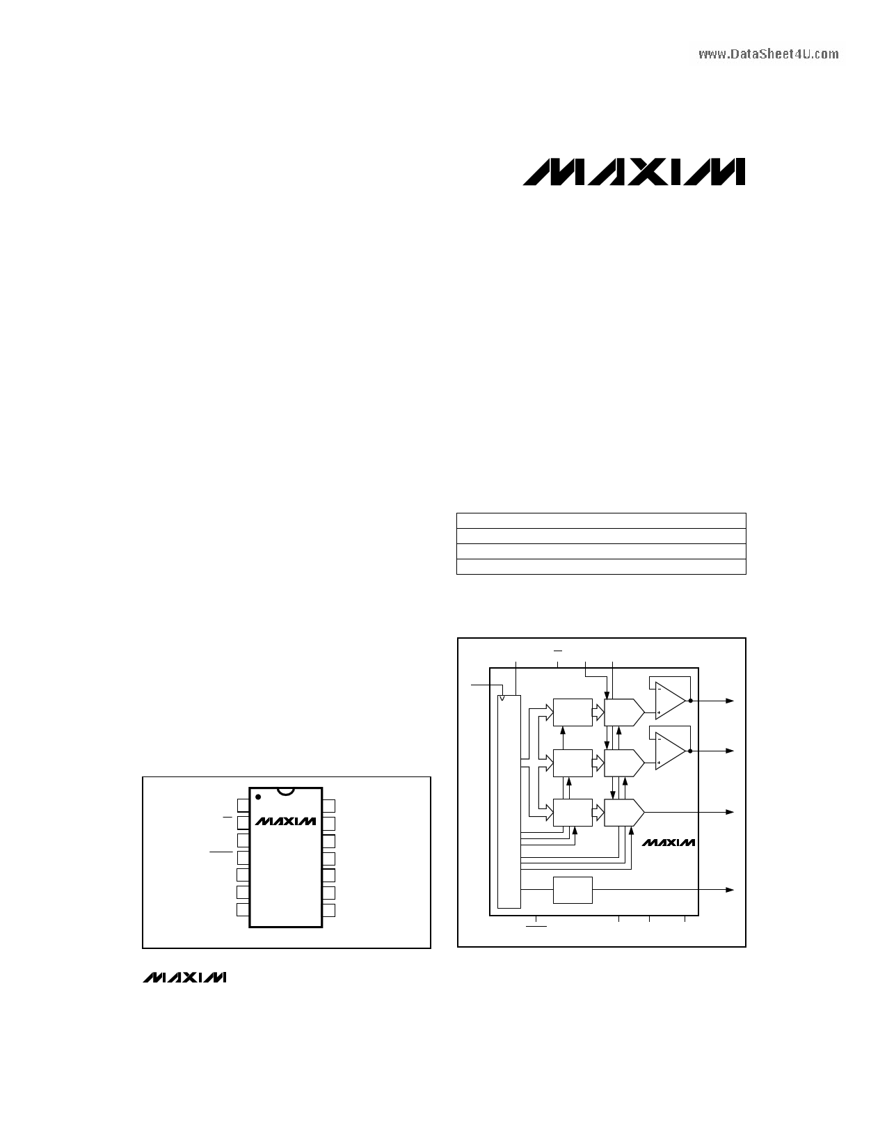
________________Functional Diagram
SCLK
3
DIN
1
CS REFAB REFC
2 12 11
DAC
LATCH
A
DAC A
DAC
LATCH
B
DAC B
OUTA
8
OUTB
9
DIN 1
CS 2
SCLK 3
RESET 4
VDD 5
GND 6
VSS 7
MAX512
MAX513
14 LOUT
13 I.C.
12 REFAB
11 REFC
10 OUTC
9 OUTB
8 OUTA
DIP/SO
DAC
LATCH
C
LATCH
4
RESET
DAC C
OUTC
10
MAX512
MAX513
LOUT
14
57
VDD VSS
6
GND
Microwire is a trademark of National Semiconductor Corp. SPI and QSPI are trademarks of Motorola Inc.
________________________________________________________________ Maxim Integrated Products 1
For free samples & the latest literature: http://www.maxim-ic.com, or phone 1-800-998-8800
1 page 
Low-Cost, Triple, 8-Bit Voltage Output DACs
with Serial Interface
____________________________Typical Operating Characteristics (continued)
(TA = +25°C, unless otherwise noted.)
SUPPLY CURRENT
vs. REFERENCE VOLTAGE
1.5
1.0 IDD, VDD = 5V, VSS = -5V
0.5 IDD, VDD = 3V, VSS = -3V
REFC GROUNDED FOR REF_ < 0
0 CODE = ALL 1s
-0.5 ISS, VDD = 3V, VSS = -3V
-1.0
ISS, VDD = 5V, VSS = -5V
-1.5
-5 -4
-3 -2 -1 0 1 2
REFAB = REFC (V)
3
REFERENCE FEEDTHROUGH
vs. FREQUENCY
0 VDD = 3V, VSS = GND = 0V
REF_ FROM 0V TO 2.9V
-20 NO LOAD
CODE = ALL 0s
4
-40
DAC C
-60
1.370
POSITIVE SUPPLY CURRENT
vs. TEMPERATURE
1.365
1.360
1.355
1.350
1.345
1.340
-60 -40 -20
VDD = +5V, VSS = GND = 0V
REFAB = REFC = VDD
ALL LOGIC INPUTS = +5V
ALL DACs SET TO ALL 1s
0 20 40 60 80 100 120 140
TEMPERATURE (°C)
REFERENCE LARGE-SIGNAL
FREQUENCY RESPONSE
5
0
-5
-10
-80
-100
www.DataSheet4U.com
-120
0.01
DAC A, B
0.1 1 10 100
FREQUENCY (kHz)
1000
-15
-20 VDD = 3V, VSS = GND = 0V
REFAB, REFC
-25 SINE WAVE 0V TO VDD
0.001 0.01 0.1 1 10 100 1000
FREQUENCY (kHz)
SHUTDOWN SUPPLY CURRENT
vs. TEMPERATURE
4.5
VDD = +5V, VSS = GND = 0V
4.0 REFAB = REFC = VDD
ALL LOGIC INPUTS = +5V
3.5
3.0
2.5
2.0
1.5
1.0
0.5
0
-60 -40 -20 0 20 40 60 80 100 120 140
TEMPERATURE (°C)
REFERENCE SMALL-SIGNAL
FREQUENCY RESPONSE
0
DAC A
-20 DAC C
DAC B
-40
-60
VDD = 3V, VSS = GND = 0V
REFAB, REFC
-80 SINE WAVE ±40mV
0.1k 1k
10k 100k
FREQUENCY (Hz)
1M
10M
_______________________________________________________________________________________ 5
5 Page 
Low-Cost, Triple, 8-Bit Voltage-Output DACs
with Serial Interface
Table 2. Serial-Interface Programming Commands
CONTROL
DATA
FUNCTION
MSB
LSB
Q2 Q1 SC SB SA LC LB LA B7 B6 B5 B4 B3 B2 B1 B0
* * * * * 0 0 0 X X X X X X X X No Operation to DAC Registers
* * * * *100
8-Bit DAC Data
Load Register to DAC C
* * * * *010
8-Bit DAC Data
Load Register to DAC B
* * * * *001
8-Bit DAC Data
Load Register to DAC A
* * * * *111
8-Bit DAC Data
Load All DAC Registers
* * 0 0 0 * * * X X X X X X X X All DACs Active
* * 1 0 0 * * * X X X X X X X X Shut Down DAC C
* * 0 1 0 * * * X X X X X X X X Shut Down DAC B
* * 0 0 1 * * * X X X X X X X X Shut Down DAC A
* * 1 1 1 * * * X X X X X X X X Shut Down All DACs
X 0 * * * * * * X X X X X X X X Reset LOUT
X 1 * * * * * * X X X X X X X X Set LOUT
X Don’t care.
* Not shown for clarity. The functions of loading and shutting down the DACs and programming the logic can be combined in a single command.
Serial-Input Data Format and Control Codes
Table 2 lists the serial-input data format. The 16-bit
input word consists of an 8-bit control byte and an 8-bit
data byte. The 8-bit control byte is not decoded inter-
nally. Every control bit performs one function. Data is
clocked in starting with Q2 (uncommitted bit), followed
by the remaining control bits and the data byte. The
www.DataSheet4U.LcSoBmof the data byte (B0) is the last bit clocked into the
shift register (Figure 2).
Example of a 16-bit input word:
Loaded
in First
Loaded
in Last
Q2 Q1 SC SB SA LC LB LA B7 B6 B5 B4 B3 B2 B1 B0
X010001110000000
The example above performs the following functions:
• 80hex (128 decimal) loaded into DAC registers
A and B.
• Content of the DAC C register remains unchanged.
• DAC A and DAC B are active.
• DAC C is shut down.
• LOUT is reset to 0.
Digital Inputs
The digital inputs are compatible with CMOS logic.
Supply current increases slightly when toggling the
logic inputs through the transition zone between
(0.3)(VDD) and (0.7)(VDD).
Digital Output
The latched digital output (LOUT) has a 1.6mA source
capability while maintaining a (VDD - 0.4V) output level.
With a 1.6mA sink current, the output voltage is guaran-
teed to be no more than 0.4V. The output can be used
for digital auxiliary control. Please note that the digital
output remains fully active during shutdown mode.
Microprocessor Interfacing
The MAX512/MAX513 serial interface is compatible with
Microwire, SPI, and QSPI. For SPI and QSPI, clear the
CPOL and CPHA bits (CPOL = 0 and CPHA = 0).
CPOL = 0 sets the inactive state of clock to zero and
CPHA = 0 changes data at the falling edge of SCLK.
This setting allows both SPI and QSPI to run at full clock
speeds (0.5MHz and 4MHz, respectively). If a serial port
is not available on your µP, three bits of a parallel port
can be used to emulate a serial port by bit manipulation.
Minimize digital feedthrough at the voltage outputs by
operating the serial clock only when necessary.
______________________________________________________________________________________ 11
11 Page | ||
| Páginas | Total 16 Páginas | |
| PDF Descargar | [ Datasheet 513CS.PDF ] | |
Hoja de datos destacado
| Número de pieza | Descripción | Fabricantes |
| 513CS | MAX513 | Maxim Integrated Products |
| Número de pieza | Descripción | Fabricantes |
| SLA6805M | High Voltage 3 phase Motor Driver IC. |
Sanken |
| SDC1742 | 12- and 14-Bit Hybrid Synchro / Resolver-to-Digital Converters. |
Analog Devices |
|
DataSheet.es es una pagina web que funciona como un repositorio de manuales o hoja de datos de muchos de los productos más populares, |
| DataSheet.es | 2020 | Privacy Policy | Contacto | Buscar |