|
|
|
PDF NJW1503A Data sheet ( Hoja de datos )
| Número de pieza | NJW1503A | |
| Descripción | Others / SSOP16 | |
| Fabricantes | JRC | |
| Logotipo | ||
Hay una vista previa y un enlace de descarga de NJW1503A (archivo pdf) en la parte inferior de esta página. Total 9 Páginas | ||
|
No Preview Available !
NJW1503A
www.DataSheet4U.com
PLL Synthesizer with 3-Wire Bus for TV Tuner
DESCRIPTION
The NJW1503A is a PLL frequency synthesizer especially designed
for TV and VCR tuning systems and consists of PLL circuit and a
prescaler which operates up to 1.0GHz, built into one chip.
The NJW1503A is controlled through a 3-wire bus.
FEATURES
• Operating Voltage 5V
• Low Operating Current : 15mA typ. @Vcc=5V
• Prescaler accepts frequencies up to 1GHz on chip
• 3-wire bus controlled
• Reference divider ratio automatic setting (512 or 1024)
• 34V max. tuning voltage output
• Package Outline: SSOP16
PACKAGE OUTLINE
NJW1503AV
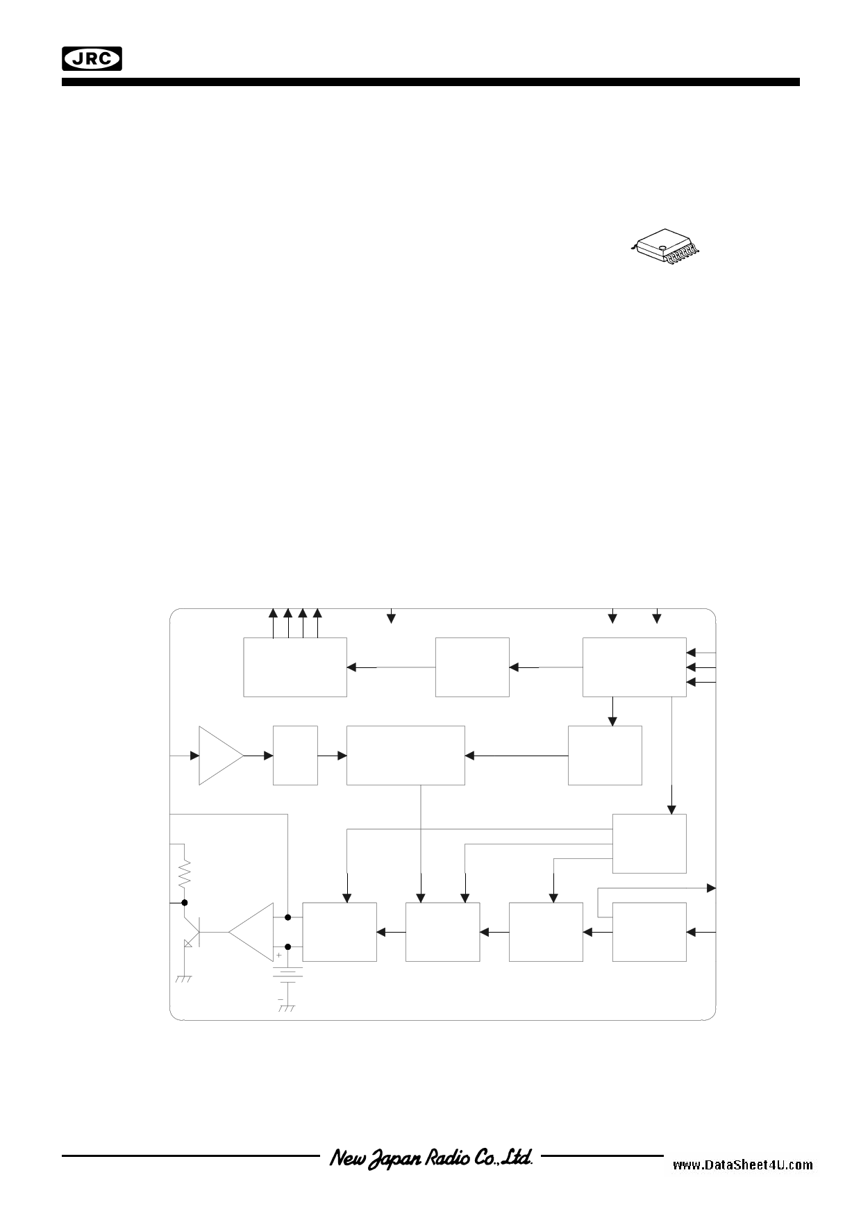
BLOCK DIAGRAM
BS0-BS3
VCC3
BAND SW
4bit
4bit
Latch
VCC1
5V GND
3Wire Bus
Receiver
CS
DAT
CLK
HF IN
CP
VCC2
PreAMP
1/8
Programmable
Divider 15bit
AMPOUT
AMP
Phase
OUT
Phase
Comp
15bit
Latch
8bit
Latch
1/1024
1/512
(1/640)
Ref
Divider
X’tal
OSC
OSCOUT
XTAL
-1-
1 page 
www.DataSheet4U.com
Serial Bus Data Format (3-Wire bus)
1. Bus protocol for18bit
B3 B2 B1 B0 N13 N12 N11 N10 N9 N8 N7 N6 N5 N4 N3 N2 N1 N0
Reference divider : fxtal 1/512
2. Bus protocol for19bit
B3 B2 B1 B0 N14 N13 N12 N11 N10 N9 N8 N7 N6 N5 N4 N3 N2 N1 N0
Reference divider : fxtal 1/1024
3. Bus protocol for Test (27bit)
B3 B2 B1 B0 N14 N13 ...N1 N0 T7 T6 T5 T4 T3 T2 T1 T0
B0 to B3 : Control of Band Switch
N0 to N14 : Control of Programmable Divider
N14=MSB N0=LSB
Division ratio : N=214×N14+213× N13+······+21×N1+N0
Maximum division ratio 32767
Minimum division ratio 256
T0 to T7 : Control bit of test
Bit T0: Charge Pump Current
T0
Charge Pump Current
Conditions
0
280uA
Normal, Default
1 60uA
Test
Bit T1 and T2: Output function of Phase Comparator
T2 T1
00
01
Phase Comparator
Normal Operation
Source
11
10
High Impedance
Sink
Conditions
Normal, Default
Test
Test
Test
Bit T4: Band Switch Test
T4 Band Switch
0 Normal Operation
1 Test
Conditions
Normal, Default
Test
Bit T5 and T6: Reference Divider
T6 T5
00
01
1*
Reference Divider
1/512
1/1024
1/640
Condition
Normal, Default
* : don’t care; 0 or 1
The 18bit and 19bit is automatic selector of the reference divider.
T3: unassigned, undefined
(Note)
Default : Power on reset
NJW1503A
-5-
5 Page | ||
| Páginas | Total 9 Páginas | |
| PDF Descargar | [ Datasheet NJW1503A.PDF ] | |
Hoja de datos destacado
| Número de pieza | Descripción | Fabricantes |
| NJW1503A | Others / SSOP16 | JRC |
| Número de pieza | Descripción | Fabricantes |
| SLA6805M | High Voltage 3 phase Motor Driver IC. |
Sanken |
| SDC1742 | 12- and 14-Bit Hybrid Synchro / Resolver-to-Digital Converters. |
Analog Devices |
|
DataSheet.es es una pagina web que funciona como un repositorio de manuales o hoja de datos de muchos de los productos más populares, |
| DataSheet.es | 2020 | Privacy Policy | Contacto | Buscar |