|
|
|
PDF STA335BWS Data sheet ( Hoja de datos )
| Número de pieza | STA335BWS | |
| Descripción | 2.1-channel high-efficiency digital audio system | |
| Fabricantes | STMicroelectronics | |
| Logotipo | ||
Hay una vista previa y un enlace de descarga de STA335BWS (archivo pdf) en la parte inferior de esta página. Total 30 Páginas | ||
|
No Preview Available !
STA335BWS
www.datasheet4u.com
2.1-channel high-efficiency digital audio system
Features
! Wide supply voltage range
– 4.5 V to 21.5 V operating
– 24 V absolute maximum rating
! Three power-output configurations
– 2-channel ternary PWM (stereo mode)
(2 x 20 W into 8 Ω at 18 V)
– 3-channel (left, right using binary and LFE)
ternary PWM (2.1 mode) (2 x 9 W +
1 x 20 W into 2 x 4 Ω, 1 x 8 Ω at 18 V)
– 2-channel ternary PWM (2 x 20 W) +
stereo lineout ternary
! 2.1 channels of 24-bit DDX®
! 100 dB SNR and dynamic range
! Selectable 32 kHz to 192 kHz input sample
rates
! I2C control with selectable device address
! Digital gain/attenuation +48 dB to -80 dB in
0.5 dB steps
! Software volume update
! Individual channel and master gain/attenuation
! Dual independent limiters/compressors
! Dynamic range compression or anti-clipping
modes
! Automodes
– 15 preset cross-over filters
– 5 preset anti-clipping modes
– Preset night-time listening mode
! Individual channel and master software and
hardware mute
! Independent channel volume and DSP bypass
! Automatic zero-detect mute
! Automatic invalid input detect mute
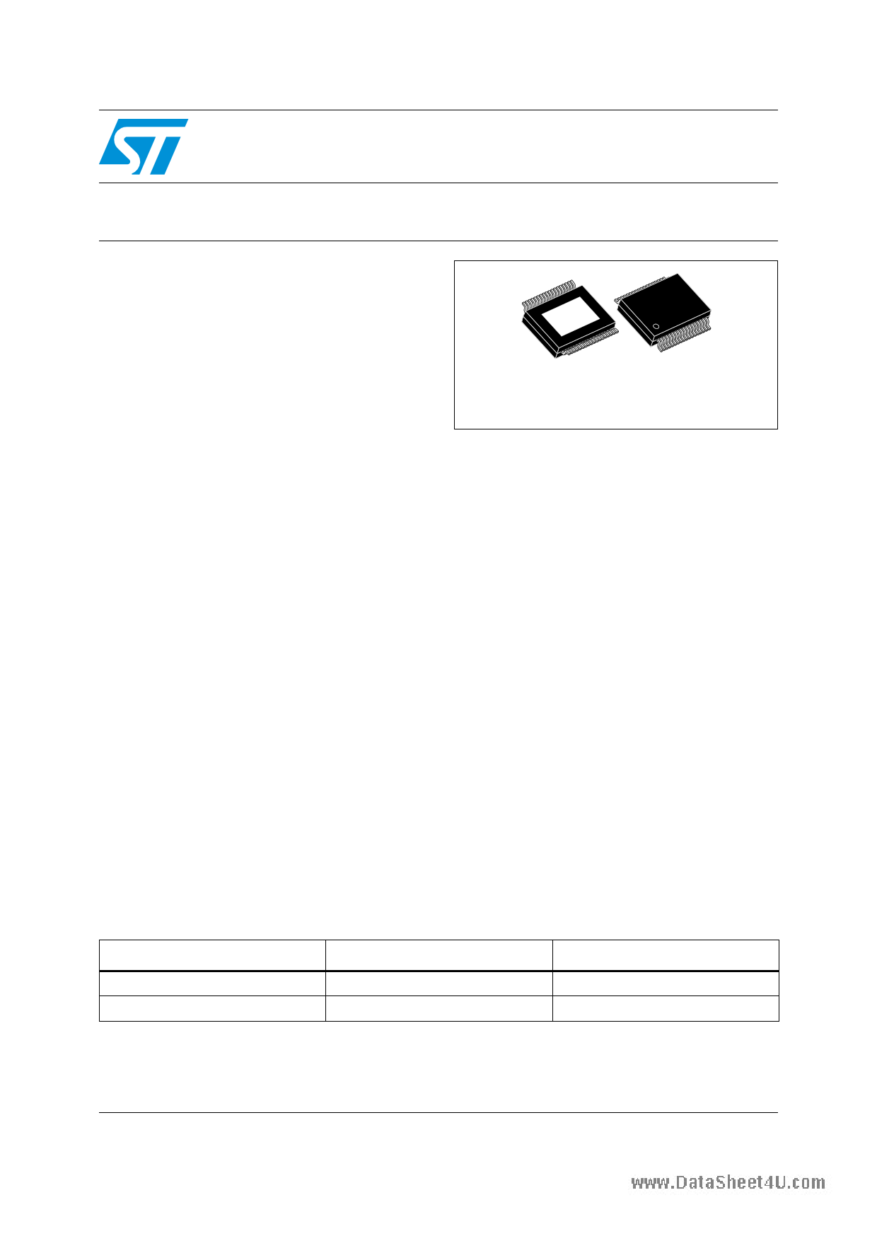
PowerSSO-36
Exposed pad down
! 2-channel I2S input data interface
! Input and output channel mapping
! 4 x 28-bit user programmable biquads (EQ) per
channel
! Up to 3 different EQ coefficients settings can
be stored and selected using I2C interface
! Bass/treble tone control
! DC-blocking selectable high-pass filter
! Selectable de-emphasis
! Sub channel mix into left and right channels
! Advanced AM interference frequency
switching and noise-suppression modes
! Selectable high or low-bandwidth
noise-shaping topologies
! Variable max power correction for lower
full-power THD
! Selectable clock input ratio
! 96 kHz internal processing sample rate,
24 to 28-bit precision
! Thermal overload and short-circuit protection
embedded
! Video application: 576 x fs input mode
supported
! PowerSSO-36 exposed pad down package
Figure 1. Device summary
Order code
STA335BWS
STA335BWS13TR
Package
PowerSSO-36 exposed pad down
PowerSSO-36 exposed pad down
Packaging
Tube
Tape and reel
January 2008
Rev 1
1/68
www.st.com
1
1 page 
STA335BWS
Contents
www.datasheet4u.com
6.12
6.13
6.14
6.15
6.16
6.17
User-defined coefficient control registers (addr 0x16 to 0x26) . . . . . . . . . 52
6.12.1 Coefficient address register . . . . . . . . . . . . . . . . . . . . . . . . . . . . . . . . . . 52
6.12.2 Coefficient b1 data register bits 23:16 . . . . . . . . . . . . . . . . . . . . . . . . . . 52
6.12.3 Coefficient b1 data register bits 15:8 . . . . . . . . . . . . . . . . . . . . . . . . . . . 53
6.12.4 Coefficient b1 data register bits 7:0 . . . . . . . . . . . . . . . . . . . . . . . . . . . . 53
6.12.5 Coefficient b2 data register bits 23:16 . . . . . . . . . . . . . . . . . . . . . . . . . . 53
6.12.6 Coefficient b2 data register bits 15:8 . . . . . . . . . . . . . . . . . . . . . . . . . . . 53
6.12.7 Coefficient b2 data register bits 7:0 . . . . . . . . . . . . . . . . . . . . . . . . . . . . 53
6.12.8 Coefficient a1 data register bits 23:16 . . . . . . . . . . . . . . . . . . . . . . . . . . 53
6.12.9 Coefficient a1 data register bits 15:8 . . . . . . . . . . . . . . . . . . . . . . . . . . . 53
6.12.10 Coefficient a1 data register bits 7:0 . . . . . . . . . . . . . . . . . . . . . . . . . . . . 54
6.12.11 Coefficient a2 data register bits 23:16 . . . . . . . . . . . . . . . . . . . . . . . . . . 54
6.12.12 Coefficient a2 data register bits 15:8 . . . . . . . . . . . . . . . . . . . . . . . . . . . 54
6.12.13 Coefficient a2 data register bits 7:0 . . . . . . . . . . . . . . . . . . . . . . . . . . . . 54
6.12.14 Coefficient b0 data register bits 23:16 . . . . . . . . . . . . . . . . . . . . . . . . . . 54
6.12.15 Coefficient b0 data register bits 15:8 . . . . . . . . . . . . . . . . . . . . . . . . . . . 54
6.12.16 Coefficient b0 data register bits 7:0 . . . . . . . . . . . . . . . . . . . . . . . . . . . . 54
6.12.17 Coefficient write/read control register . . . . . . . . . . . . . . . . . . . . . . . . . . 55
6.12.18 User-defined EQ . . . . . . . . . . . . . . . . . . . . . . . . . . . . . . . . . . . . . . . . . . 57
6.12.19 Pre-scale . . . . . . . . . . . . . . . . . . . . . . . . . . . . . . . . . . . . . . . . . . . . . . . . 57
6.12.20 Post-scale . . . . . . . . . . . . . . . . . . . . . . . . . . . . . . . . . . . . . . . . . . . . . . . 57
6.12.21 Over-current post-scale . . . . . . . . . . . . . . . . . . . . . . . . . . . . . . . . . . . . . 58
Variable max power correction registers (addr 0x27 to 0x28) . . . . . . . . . 59
Variable distortion compensation registers (addr 0x29 to 0x2A) . . . . . . . 59
Fault detect recovery constant registers (addr 0x2B to 0x2C) . . . . . . . . . 60
Device status register (addr 0x2D) . . . . . . . . . . . . . . . . . . . . . . . . . . . . . . 60
EQ coefficients and DRC configuration register (addr 0x31) . . . . . . . . . . 61
7 Application . . . . . . . . . . . . . . . . . . . . . . . . . . . . . . . . . . . . . . . . . . . . . . . . 62
7.1 Application schematic and power supplies . . . . . . . . . . . . . . . . . . . . . . . . 62
7.2 PLL filter schematic . . . . . . . . . . . . . . . . . . . . . . . . . . . . . . . . . . . . . . . . . 62
7.3 Typical output configuration . . . . . . . . . . . . . . . . . . . . . . . . . . . . . . . . . . . 63
8 Package thermal characteristics . . . . . . . . . . . . . . . . . . . . . . . . . . . . . . 64
9 Package information . . . . . . . . . . . . . . . . . . . . . . . . . . . . . . . . . . . . . . . . 65
5/68
5 Page 
STA335BWS
Connection diagram and pin description
2 Connection diagram and pin description
2.1
www.datasheet4u.com
Connection diagram
Figure 3. Pin connection PowerSSO-36 (Top view)
GND_SUB
SA
TEST_MODE
VSS
VCC_REG
OUT2B
GND2
VCC2
OUT2A
OUT1B
VCC1
GND1
OUT1A
GND_REG
VDD
CONFIG
OUT3B/DDX3B
OUT3A/DDX3A
1
2
3
4
5
6
7
8
9
10
11
12
13
14
15
16
17
18
36 VDD_DIG
35 GND_DIG
34 SCL
33 SDA
32 INT_LINE
31 RESET
30 SDI
29 LRCKI
28 BICKI
27 XTI
26 PLL_GND
25 FILTER_PLL
24 VDD_PLL
23 PWRDN
22 GND_DIG
21 VDD_DIG
20 TWARN/OUT4B
19 EAPD/OUT4A
D05AU1638
2.2
Pin description
Table 1.
Pin
1
2
3
4
5
6
7
8
Pin description
Type
Name
GND
GND_SUB
I SA
I TEST_MODE
I/O VSS
I/O Vcc_REG
O OUT2B
GND
GND2
Power
VCC2
Description
Substrate ground
I2C select address
This pin must be connected to ground
Internal reference at Vcc - 3.3 V
Internal Vcc reference
Output half bridge 2B
Power negative supply
Power positive supply
11/68
11 Page | ||
| Páginas | Total 30 Páginas | |
| PDF Descargar | [ Datasheet STA335BWS.PDF ] | |
Hoja de datos destacado
| Número de pieza | Descripción | Fabricantes |
| STA335BW | 2.1 channels high efficiency digital audio system | STMicroelectronics |
| STA335BWQS | 2.1-channel high-efficiency digital audio system | STMicroelectronics |
| STA335BWS | 2.1-channel high-efficiency digital audio system | STMicroelectronics |
| STA335BWSQS | high-efficiency digital audio system | ST Microelectronics |
| Número de pieza | Descripción | Fabricantes |
| SLA6805M | High Voltage 3 phase Motor Driver IC. |
Sanken |
| SDC1742 | 12- and 14-Bit Hybrid Synchro / Resolver-to-Digital Converters. |
Analog Devices |
|
DataSheet.es es una pagina web que funciona como un repositorio de manuales o hoja de datos de muchos de los productos más populares, |
| DataSheet.es | 2020 | Privacy Policy | Contacto | Buscar |