|
|
|
PDF ACS8522A Data sheet ( Hoja de datos )
| Número de pieza | ACS8522A | |
| Descripción | Synchronous Equipment Timing Source | |
| Fabricantes | Semtech Corporation | |
| Logotipo | ||
Hay una vista previa y un enlace de descarga de ACS8522A (archivo pdf) en la parte inferior de esta página. Total 30 Páginas | ||
|
No Preview Available !
ACS8522A SETS LITE
Synchronous Equipment Timing Source for
Stratum 3/4E/4 and SMC Systems
ADVANCED COMMSUN&ICSAETNIOSNINSG
Deswcwrwi.pDattiaoSnheet4U.com
FINAL
Features
DATASHEET
The ACS8522A is a highly integrated, single-chip solution for the
Synchronous Equipment Timing Source (SETS) function in a
SONET or SDH Network Element. The device generates SONET
or SDH Equipment Clocks (SEC) and Frame Synchronization
clocks. The ACS8522A is fully compliant with the required
international specifications and standards.
Suitable for Stratum 3, 4E, 4 and SONET Minimum
Clock (SMC) or SONET/SDH Equipment Clock (SEC)
applications (to Telcordia 1244-CORE[19] Stratum 3
and GR-253[17], and ITU-T G.813[11] Options Ι and ΙΙ
specifications).
The device supports Free-run, Locked and Holdover modes,
with mode selection controlled either automatically by an
internal state machine or forced by register configuration.
The ACS8522A accepts up to four independent input SEC
reference clock sources from Recovered Line Clock, PDH
network, and Node Synchronization. The ACS8522A generates
independent SEC and BITS clocks, an 8 kHz Frame
Synchronization clock and a 2 kHz Multi-Frame Synchronization
clock, both with programmable pulse width and polarity.
The ACS8522A includes a Serial Port, which can be SPI
compatible, providing access to the configuration and status
registers for device setup.
The ACS8522A supports IEEE 1149.1[5] JTAG boundary scan.
The User can choose between OCXO or TCXO to define the
Stratum and/or Holdover performance required.
Accepts four individual input reference clocks, all with
robust input clock source quality monitoring.
Simultaneously generates four output clocks, plus two
Sync pulse outputs.
Absolute Holdover accuracy better than 3 x 10⁻¹⁰
(manual), 7.5 x 10⁻¹⁴ (instantaneous); Holdover
stability defined by choice of external XO.
Programmable PLL bandwidth, for wander and jitter
tracking/attenuation, 0.1 Hz to 70 Hz in 10 steps.
Automatic hit-less source switchover on loss of input
Serial SPI compatible interface.
Output phase adjustment in 6 ps steps up to ±200 ns
IEEE 1149.1[5] JTAG Boundary Scan.
Available in LQFP 64-pin package.
Single 3.3 V operation.
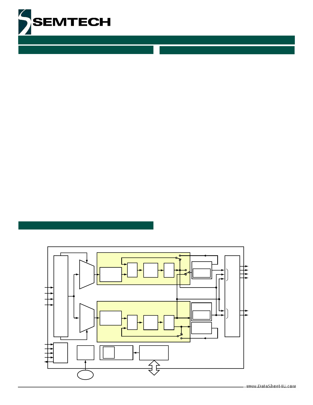
Block Diagram
Lead (Pb)-free version available (ACS8522AT), RoHS
and WEEE compliant.
Figure 1 Block Diagram of the ACS8522A SETS LITE
Inputs: 4 x TTL
Programmable;
2 kHz
4 kHz
N x 8 kHz
1.544/2.048 MHz
6.48 MHz
19.44 MHz
25.92 MHz
38.88 MHz
51.84 MHz
77.76 MHz
Input
Port
Monitors
and
Selection
Control
4 x SEC
T4 DPLL
Selector
T4 DPLL/Freq. Synthesis
Digital
Optional
Divider, 1/n
n = 1 to 214
PFD
Loop
Filter
DTO
T0 DPLL
Selector
T0 DPLL/Freq. Synthesis
Optional
Divider, 1/n
n = 1 to 214
PFD
Digital
Loop
Filter
DTO
TCK
TDI
TMS
TRST
TDO
IEEE
1149.1
JTAG
Chip
Clock
Generator
Priority Register Set
Table
OCXO or
TCXO
Revision 1.00/September 2007 © Semtech Corp.
Serial
Port
Page 1
T4 Output
APLL
Frequency
Dividers
T0 Output
APLL
Frequency
Dividers
T0 Feedback
APLL
Output
Ports
O1
to
O4
Output O1: PECL/LVDS
Outputs O2 - 04: TTL
Programmable;
E1/DS1 (2.048/
1.544 MHz)
and frequency
multiples:
1.5 x, 2 x, 3 x
4 x, 6 x, 12 x
16 x and 24 x
E3/DS3
2 kHz
8 kHz
and OC-N* rates
FrSync
&
MFrSync
8 kHz
(FrSync)
2 kHz
(MFrSync)
OC-N* rates =
OC-1 51.84 MHz
OC-3 155.52 MHz
and derivatives:
6.48 MHz
19.44 MHz
25.92 MHz
38.88 MHz
51.84 MHz
77.76 MHz
155.52 MHz
311.04 MHz
F8522P_001BLOCKDIA_04
www.semtech.com
1 page 
ACS8522A SETS LITE
ADVANCED COMMS & SENSING
PinwDwwe.DsactarSipheteito4Un.com
Table 1 Power Pins
Pin Number
Symbol
8, 9, VD1+, VD2+,
12 VD3+
22 VDD_DIFF
I/O
P
P
Type
-
-
27
VDDCLMP
P
-
32, 36,
38, 39,
45, 46,
54
4
VDD1, VDD2,
VDD3, VDD4,
VDD5, VDD6,
VDD7
VA1+
P
P
-
-
14, 57
VA2+, VA3+
P
-
15, 58
7, 10,
11
31, 40,
53
21
1, 3
AGND3, AGND4
DGND1, DGND2,
DGND3
DGND4, DGND5,
DGND6
GND_DIFF
AGND1, AGND2
P
P
P
P
-
-
-
-
-
FINAL
DATASHEET
Description
Supply Voltage: Digital supply to gates in analog section, +3.3 Volts
±5%.
Supply Voltage: Digital supply for differential output pins 19 and 20,
+3.3 Volts ±5%.
Digital Supply for input over-voltage clamping to +3.3 volts. Leave
floating for no clamping.
Supply Voltage: Digital supply to logic, +3.3 Volts ±5%.
Supply Voltage: Analog supply to clock multiplying PLL,
+3.3 Volts ±5%.
Supply Voltage: Analog supply to output PLLs APLL2 and APLL1,
+3.3 Volts ±5%.
Supply Ground: Analog ground for output PLLs APLL2 and APLL1.
Supply Ground: Digital ground for components in PLLs.
Supply Ground: Digital ground for logic.
Supply Ground: Digital ground for differential output pins 19 and 20.
Supply Ground: Analog grounds.
Note...I = Input, O = Output, P = Power, TTLU = TTL input with pull-up resistor, TTLD = TTL input with pull-down resistor.
Table 2 Internally Connected Pins
Pin Number
Symbol
2, 16, 23, 24,
25, 26, 35,
60, 61, 62,
63
IC1, IC2, IC3, IC4,
IC5, IC6, IC7,
IC8, IC9, IC10,
IC11
I/O
-
Type
-
Description
Internally Connected: Leave to Float.
Table 3 Other Pins
Pin Number
Symbol
5 INTREQ
6 REFCLK
13 SRCSW
I/O
O
I
I
Type
TTL/CMOS
TTL
TTLD
Description
Interrupt Request: Active High/Low software Interrupt output.
Reference Clock: 12.800 MHz (refer to section headed Local Oscillator
Clock).
Source Switching: Force Fast Source Switching on SEC1 and SEC2.
Revision 1.00/September 2007 © Semtech Corp.
Page 5
www.semtech.com
5 Page 
ACS8522A SETS LITE
ADVANCED COMMS & SENSING
FINAL
DATASHEET
beenwrwawis.Deadta,Sthheeent4Uth.ceomDPLL will continue to lock to the
input, with little disturbance. In this scenario, with the
DPLL in the “locked” state, the DPLL uses “nearest edge
locking” mode (±180° capture) avoiding cycle slips or
glitches caused by trying to lock to an edge 360° away, as
Each source is monitored over a 128 ms period. If, within
a 128 ms period, an irregularity occurs that is not deemed
to be due to allowable jitter/wander, then the
Accumulator is incremented.
would happen with traditional PLLs.
The Accumulator will continue to increment up to the
point that it reaches the programmed Bucket size. The “fill
Activity Monitoring
The ACS8522A has a combined inactivity and irregularity
monitor. The ACS8522A uses a Leaky Bucket
Accumulator, which is a digital circuit which mimics the
operation of an analog integrator, in which input pulses
increase the output amplitude but die away over time.
Such integrators are used when alarms have to be
rate” of the Leaky Bucket is, therefore, 8 units/second.
The “leak rate” of the Leaky Bucket is programmable to
be in multiples of the fill rate (x 1, x 0.5, x 0.25 and
x 0.125) to give a programmable leak rate from
8 units/sec down to 1 unit/sec. A conflict between trying
to “leak” at the same time as a “fill” is avoided by
preventing a leak when a fill event occurs.
triggered either by fairly regular defect events, which
occur sufficiently close together, or by defect events
which occur in bursts. Events which are sufficiently
spread out should not trigger the alarm. By adjusting the
alarm setting threshold, the point at which the alarm is
triggered can be controlled. The point at which the alarm
is cleared depends upon the decay rate and the alarm
clearing threshold.
Disqualification of a non-selected reference source is
based on inactivity, or on an out-of-band result from the
frequency monitors. The currently selected reference
source can be disqualified for phase, frequency, inactivity
or if the source is outside the DPLL lock range. If the
currently selected reference source is disqualified, the
next highest priority, qualified reference source is
selected.
On the alarm setting side, if several events occur close
together, each event adds to the amplitude and the alarm
will be triggered quickly; if events occur further apart, but
still sufficiently close together to overcome the decay, the
alarm will be triggered eventually. If events occur at a rate
which is not sufficient to overcome the decay, the alarm
will not be triggered. On the alarm clearing side, if no
defect events occur for a sufficient time, the amplitude
Interrupts for Activity Monitors
The loss of the currently selected reference source will
eventually cause the input to be considered invalid,
triggering an interrupt, if not masked. The time taken to
raise this interrupt is dependent on the Leaky Bucket
Configuration of the activity monitors. The fastest Leaky
will decay gradually and the alarm will be cleared when Bucket setting will still take up to 128 ms to trigger the
the amplitude falls below the alarm clearing threshold.
The ability to decay the amplitude over time allows the
importance of defect events to be reduced as time passes
by. This means that, in the case of isolated events, the
alarm will not be set, whereas, once the alarm becomes
set, it will be held on until normal operation has persisted
for a suitable time (but if the operation is still erratic, the
alarm will remain set). See Figure 3.
interrupt. The interrupt caused by the brief loss of the
currently selected reference source is provided to
facilitate very fast source failure detection if desired. It is
triggered after missing just a couple of cycles of the
reference source. Some applications require the facility to
switch downstream devices based on the status of the
reference sources. In order to provide extra flexibility, it is
possible to flag the main_ref_failed interrupt (Reg. 06 Bit
There is one Leaky Bucket Accumulator per input channel.
Each Leaky Bucket can select from four Configurations
(Leaky Bucket Configuration 0 to 3). Each Leaky Bucket
Configuration is programmable for size, alarm set and
6) on the pin TDO. This is simply a copy of the status bit in
the interrupt register and is independent of the mask
register settings. The bit is reset by writing to the interrupt
status register in the normal way. This feature can be
reset thresholds, and decay rate.
enabled and disabled by writing to Reg. 48 Bit 6.
Revision 1.00/September 2007 © Semtech Corp.
Page 11
www.semtech.com
11 Page | ||
| Páginas | Total 30 Páginas | |
| PDF Descargar | [ Datasheet ACS8522A.PDF ] | |
Hoja de datos destacado
| Número de pieza | Descripción | Fabricantes |
| ACS8522 | Synchronous Equipment Timing Source | Semtech Corporation |
| ACS8522A | Synchronous Equipment Timing Source | Semtech Corporation |
| Número de pieza | Descripción | Fabricantes |
| SLA6805M | High Voltage 3 phase Motor Driver IC. |
Sanken |
| SDC1742 | 12- and 14-Bit Hybrid Synchro / Resolver-to-Digital Converters. |
Analog Devices |
|
DataSheet.es es una pagina web que funciona como un repositorio de manuales o hoja de datos de muchos de los productos más populares, |
| DataSheet.es | 2020 | Privacy Policy | Contacto | Buscar |