|
|
|
PDF STV9380A Data sheet ( Hoja de datos )
| Número de pieza | STV9380A | |
| Descripción | CLASS-D VERTICAL DEFLECTION AMPLIFIER | |
| Fabricantes | STMicroelectronics | |
| Logotipo | ||
Hay una vista previa y un enlace de descarga de STV9380A (archivo pdf) en la parte inferior de esta página. Total 10 Páginas | ||
|
No Preview Available !
® STV9380A
Class-D Vertical Deflection Amplifier
for 2.5 Amp TV and Monitor Applications
Main Features
s High-Efficiency Power Amplifier
s No Heatsink
www.DatasSheSet4pUli.ctoSmupply
s Internal Flyback Generator
s Output Current up to 2.5 APP
s Suitable for DC Coupling Applications
s Few External Components
s Protection against Low VCC
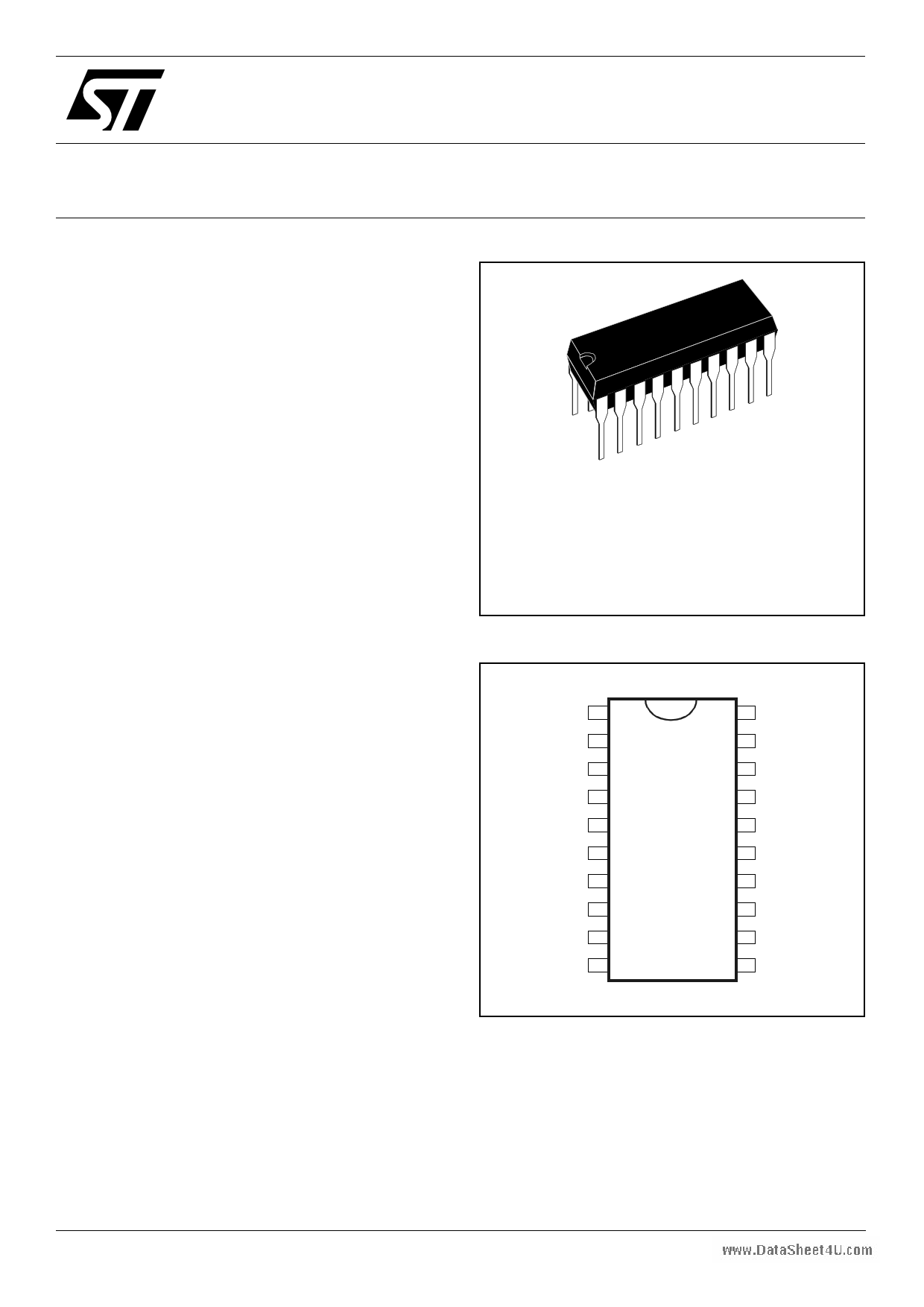
PDIP 20
Order Code: STV9380A
Description
Designed for TV and monitor applications, the
STV9380A is a Class-D vertical deflection booster
assembled in a 20-pin plastic DIP package.
It operates with supplies up to ±18 V and provides
an output current up to 2.5 APP to drive the yoke.
The internal flyback generator avoids the need for
an extra power supply.
-VCC
-VCC
-VCC
OUT
CFLY +
CFLY -
BOOT
VREG
FEEDCAP
FREQ
1
2
3
4
5
6
7
8
9
10
20 -VCC
19 -VCC
18 -VCC
17 -VCC POW
16 + VCC POW
15 +VCC
14 EAout
13 IN+
12 IN-
11 SGND
October 2003
1/10
This is preliminary information on a new product now in development or undergoing evaluation. Details are subject to change without notice.
1 page 
STV9380A
5 Electrical Characteristics
Electrical Characteristics
TAMB = 25° C, VCC = ±12 V and fVERT = 50 Hz unless otherwise specified (refer to Figure 1)
Symbol
Parameter
+VCC Positive Supply Range
-VCC
Negative Supply Range
∆VCC
www.DataSheet4U.com
VCCSTART
Maximum recommended difference
between +VCC and |-VCC|
Low VCC Detection
IQ Quiescent Supply Current
IY Maximum Vertical Yoke Current
I13, I12 Amplifier Input Bias Current
VOS Output Offset Voltage
SVR Supply Voltage Rejection
FlyTHR
Flyback Detection Threshold
(Positive Slope)
FlyTHF
Flyback Detection Threshold
(Negative Slope)
PD
Integrated Circuit
Dissipated Power
fSW Switching Frequency
fSW-OP Switching Frequency Operative Range
RFREQ Frequency Controller Resistor Range
Test Conditions
Input Voltage = 0
Note 1
Note 2
V(14)
V(14)
Note 3
RFREQ = 10 kΩ
Pin 10
Min.
+10
-18
-50
120
100
7
Typ.
±6.5
14
-0.1
82
1.5
0.5
1.1
140
10
Max.
+18
-10
±4
±1.25
+50
Units
V
V
V
V
mA
A
µA
mV
dB
V
V
W
160 kHz
200 kHz
14 kΩ
Note 1. Input voltage = 0, measured after the filter (e.g. across the 470 nF filter capacitor)
2. Supply rejection of the positive or negative power supply. VCC ripple =1 VPP , f =100 Hz, measured
on the sense resistor.
3. Power dissipated in the circuit in the case of the application from Figure 1 and the current in the
deflection yoke adjusted to 2.5 APP. The corresponding power dissipated in the vertical deflection
yoke is 2.8 W.
5/10
5 Page | ||
| Páginas | Total 10 Páginas | |
| PDF Descargar | [ Datasheet STV9380A.PDF ] | |
Hoja de datos destacado
| Número de pieza | Descripción | Fabricantes |
| STV9380 | CLASS-D VERTICAL DEFLECTION AMPLIFIER | STMicroelectronics |
| STV9380A | CLASS-D VERTICAL DEFLECTION AMPLIFIER | STMicroelectronics |
| Número de pieza | Descripción | Fabricantes |
| SLA6805M | High Voltage 3 phase Motor Driver IC. |
Sanken |
| SDC1742 | 12- and 14-Bit Hybrid Synchro / Resolver-to-Digital Converters. |
Analog Devices |
|
DataSheet.es es una pagina web que funciona como un repositorio de manuales o hoja de datos de muchos de los productos más populares, |
| DataSheet.es | 2020 | Privacy Policy | Contacto | Buscar |